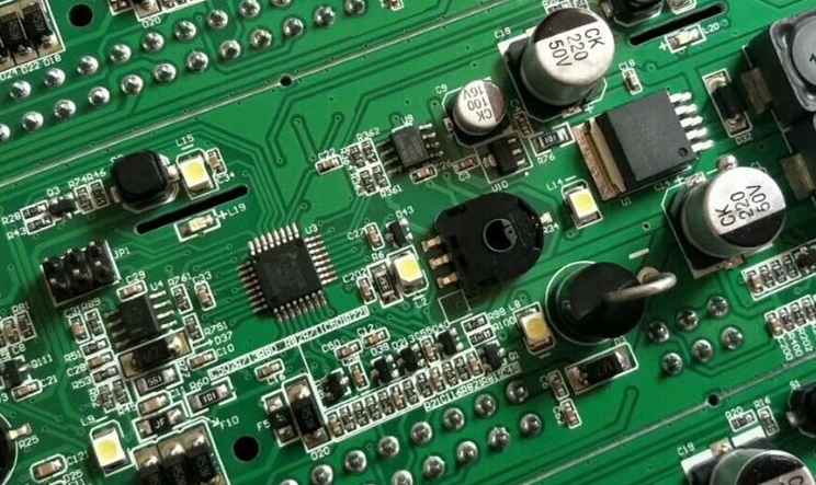
As a platform for numerous components and circuit signal transmission, Printed Circuit Boards (PCBs) have been regarded as such a key section of electronic information products that their quality determines quality and reliability of end products. Owing to uprising development trend towards high density and lead-free and halogen-free environmental requirement, if professional and timely inspection leaves undone, all kinds of failure issues possibly take place to PCBs such as bad wettability, crack, delamination etc.
In order to ensure both high quality and reliability of assembled PCBs, PCB manufacturers and assemblers have to implement inspections for boards at different stages during manufacturing and assembly procedure so that surface defects will be eliminated. Furthermore, timely and professional inspections are capable of leading defects to be exposed prior to electrical test and are beneficial for data accumulation for Statistical Process Control (SPC).
In general, PCB assembly inspection technologies are classified into two types: visual inspection and automatic process inspection.
a.Visual Inspection
Visual inspection can be used after lots of steps during PCB assembly process and equipment for visual inspection is selected based on the positions of inspection targets. For example, after solder paste printing and device placement, inspection staff is able to find out obvious defects with naked eyes such as contaminative solder paste and missing components. The most prevalent visual inspection is capable of inspecting reflow solder joints by observing light rays reflected from ordinary prism from different angles. Generally speaking, this type of inspection can test 5 joints in just one second.
b. Structural Process Test System (SPTS)
Digitalization and analysis system of real-time and automatic video capture is capable of dramatically improving allowance and repeatability of visual inspection. Therefore, structural process test system depends on some form of emitting light like visible light, laser beam and X ray. All those systems acquire information through processing images to find out and measure defects concerned with solder joint quality. Similar with visual inspection, SPTS is implemented without the need to physically contact circuit board. Different from visual inspection, however, SPTS features such high repeatability and eliminates subjectivity from defect measurement.
• Automatic/Automated Optical Inspection (AOI)
AOI system relies on multiple light sources, programmable LED library and some cameras to shine solder joints and take shots. Under reflected light, leads and solder joints play a role as mirror reflecting majority of light while both PCBs and SMDs reflect little light. Light reflected from solder joints fails to provide the practical height data while graphics and intensity of reflected light provides information in terms of solder joint curvature. Then professional analysis will take place to determine whether solder joints are complete, whether solder is sufficient, whether bad wetting takes place. Apart from that, AOI system also inspect solder bridging and missing components or displacement before or after reflow soldering.

• Automatic Laser Test (ALT) Measurement
ALT is a more direct technology used to test height and shape of solder joints or solder paste deposition. This system runs to measure the height and reflectivity of some surface components when the image of laser beam focuses on one or multiple position sensitive detectors that maintain a certain angle with laser beam. During ALT measurement, surface height is determined by the light position reflected from position sensitive detectors while surface reflectivity is figured out from the power of reflected light beam.
• X-ray Fluoroscopic System
X-ray fluoroscopic system emits a beam of rays from a single-point light source, which vertically goes through circuit board. With this process carrying on, solder joints weaken the intensity of rays to larger extent than other materials. On a single-side PCB, X-ray fluoroscopic system is capable of accurately inspecting solder joint defects such as those (including crack, insufficient solder, bridging, misalignment, void etc.) taking place on J-shape wiring devices, gull-wing devices or passive chips. Apart from that, it is able to inspect missing components and reversed tantalum capacitors. When it comes to double-side PCBs, however, X-ray fluoroscopic system fails to accurately inspect those defects due to possible overlapping of X-ray images of solder joints on both sides of a board.
• X-ray Lamination System
Compared with X-ray fluoroscopic system, X-ray lamination system generates focal plane of a horizontal section area through scanning or synchronously spinning with X-ray detector. X-ray lamination system can measure parameters of all physical solder joints at different focal planes so that process defect coverage can be provided. Due to the indicated relationship between section image of X rays and given solder paste volume, grey scale readings can be converted into practical sizes by regulated standard units or metric units. After analysis on measurement results, data will be provided to characterization and assembly improvement.X-ray lamination system features the highest cost among all inspection methods but greatly shortens time of searching and rework.
Printed Circuit Board assembly manufacturing hardly relies on single inspection method. After all, visual inspection can never be avoided during assembly procedure. Due to complexity improvement and high volume assembly demand, automatic inspection methods have to be used.
Any pending projects, please contact Unit Circuits, our website www.unitcircuits.com.
PCB supply chain management/PCB and Assembly SERVICES/EMS business/Electronic assemblies/PCB Contract Manufacturer/Rapid PCB Prototyping/Box Build service/Electronics Manufacturing/PCB Manufacturing/PCB solution/PCB Supply solution/PCB procurement.