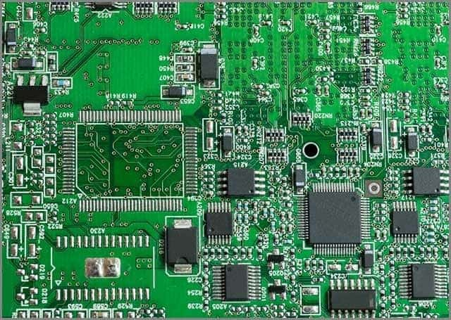
Multi-Layer PCB Assembly
High-Quality Multi-Layer PCB Assembly Services Since 2017
- Multi-Layer PCB Assembly
- Flexible Options: Consigned, Partial Turnkey, Full Turnkey
- No MOQ & Competitive Pricing
- Comprehensive Testing:E-test, AOI, X-ray, ICT, FCT, Burn-in Testing
- Certified for Quality:ISO 9001:2015, ISO 13485:2016, UL Listed
- Advanced Capabilities:Supports 0201 components, BGA, micro-BGA, QFN, DFN, CSP
- Ideal for High-Density, High-Performance Applications
- Industries We Serve: Medical, Automotive, Telecom, Industrial Equipment, and more
Multi-Layer PCB Assembly
Multi-Layer PCB Assembly refers to the process of assembling a printed circuit board (PCB) with multiple layers of conductive traces, which are laminated together to create a high-density, highly functional circuit. This type of PCB assembly is typically used in complex electronic devices where high performance, miniaturization, and signal integrity are critical. Whether you’re a beginner, a professional, or a business owner looking to outsource PCB assembly services, this guide will walk you through everything you need to know about Multi-Layer PCB Assembly.

Leading PCBA Manufacturer
Assemble 20 PCBAS for $0
What is Multi-Layer PCB Assembly?
Multi-Layer PCB Assembly is a method of constructing printed circuit boards that have more than two layers of conductive material. These layers are stacked and laminated together, with electrical connections made between them using vias. Multi-layer PCBs are essential for modern, compact, and highly functional electronic devices, including mobile phones, computers, medical equipment, and automotive systems.
Why is Multi-Layer PCB Assembly important?
This assembly method allows for the creation of complex, compact designs by stacking multiple layers of circuits. It’s ideal for applications that require high-density interconnections, better signal integrity, and advanced features, such as high-frequency signal routing and power management.
What is the Multi-Layer PCB assembly process?
The process involves stacking multiple layers of PCB material, etching traces, drilling vias, and then assembling the components onto the final multi-layered board. The layers are connected to each other through vias and plated through holes (PTH) for electrical connections.
The Benefits of Multi-Layer PCB Assembly
Multi-Layer PCB Assembly offers several significant advantages, particularly for high-performance and miniaturized electronic devices. Some key benefits include:
- 1.Higher Component Density
With multiple layers, a multi-layer PCB can accommodate a greater number of components in a smaller space, making it ideal for compact and high-performance devices.
- 2.Improved Signal Integrity
Multi-layer PCBs are essential for maintaining signal integrity, particularly in high-frequency applications. The layers can be used to isolate sensitive signals and reduce noise, ensuring better performance and reliability. - 3.Compact and Efficient Design
Multi-layer PCBs enable more efficient use of space, allowing for smaller devices with more complex functionality. This is particularly important in industries where miniaturization is critical, such as wearables and IoT devices. - 4.Better Power Management
The multiple layers provide improved power distribution and allow for better heat management, reducing the risk of power-related issues such as overheating and voltage drops. - 5.Complex Functionality in One Board
Multi-layer PCBs allow for complex circuit designs that would otherwise require multiple single or double-sided boards. This reduces overall system complexity and makes the design process more efficient.
The Main Challenges in Assembling Multi-Layer PCBs
Multi-Layer PCB Assembly presents several challenges due to the complexity of the process and the advanced technology involved. These include:
- Layer Alignment Issues
Proper alignment of multiple layers is crucial to ensure correct electrical connections between them. Misalignment can lead to faulty connections and reduced board performance. - Complex Drilling and Via Technology
Drilling holes (vias) through multiple layers to create electrical connections is a complex and precise task. Any errors in drilling can result in poor conductivity and malfunctioning boards. - Signal Integrity and Crosstalk
Multi-layer PCBs must be designed carefully to minimize issues like crosstalk and signal interference. Improper routing of signals can lead to noise and reduced performance, especially in high-frequency applications. - Heat Management
With more layers, heat dissipation becomes a greater concern. Proper thermal management solutions must be incorporated into the design to prevent overheating and damage to sensitive components. - Increased Manufacturing Complexity
Multi-layer PCB Assembly is more complex and time-consuming than single or double-sided PCBs. The process requires advanced equipment and expertise, which can increase both manufacturing time and costs.
By using the latest technologies and ensuring rigorous quality control, these challenges can be overcome, ensuring the assembly of high-quality and reliable multi-layer PCBs.
What is the Multi-Layer setup?
The Multi-Layer setup involves stacking several layers of conductive material, interconnecting them with vias, and assembling components onto these layers. This design enables complex functionality in a compact form factor.
The Key Processes in Multi-Layer PCB Assembly
Multi-Layer PCB Assembly involves several intricate steps to ensure a functional and reliable end product. These key processes include:
- 1.Layer Stacking and Lamination
The process begins by stacking multiple layers of PCB material, which are then laminated together. Each layer is etched to create traces and interconnections, with the vias drilled through the layers for electrical connections. - 2.Via Drilling and Plating
Vias (electrical connections between layers) are drilled and plated to establish electrical paths between the different layers of the PCB. This is a highly precise step to ensure reliable inter-layer connections.
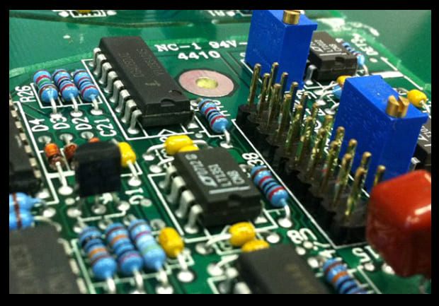
- 3.Component Placement
After the layers are connected, components are placed on the surface of the board. Surface Mount Technology (SMT) and Through-Hole Technology (THT) are both commonly used in multi-layer assembly, depending on the components and design. - 4.Soldering
The components are then soldered in place. Reflow soldering is typically used for SMT components, while Through-Hole components are soldered using wave soldering or hand soldering methods. - 5.Inspection and Testing
After assembly, the multi-layer PCB undergoes rigorous inspection to identify defects such as poor solder joints, misaligned components, or damaged traces. Electrical testing is also conducted to ensure the functionality of the board.
Why Choose Unit Circuits As Your Partner?
When it comes to Multi-Layer PCB Assembly, Unit Circuits is the partner you can trust for high-quality, reliable services. Here’s why:
- Expertise in Multi-Layer Assembly
With years of experience in Multi-Layer PCB Assembly, we possess the skills and technology to handle even the most complex designs. We specialize in both SMT and THT to meet your specific needs. - Quality Assurance
We have rigorous quality control measures in place, ensuring that every multi-layer PCB we assemble meets the highest standards for performance and reliability. - Advanced Technology
Our cutting-edge technology allows us to handle the intricate processes involved in Multi-Layer PCB Assembly, including precise layer stacking, via drilling, and complex component placement. - Cost-Effective Solutions
While multi-layer PCBs are more complex, we provide cost-effective solutions by optimizing the manufacturing process without compromising on quality, ensuring your project stays on budget. - Comprehensive Support
From design consultation to final testing, we provide full support at every stage of the assembly process, helping you achieve the best possible results for your project.
CONNECT WITH US
Get A Instant Quote Today
Unit Circuits is your trusted partner for PCB fabrication, components sourcing, and PCB assembly. With over 7 years of experience, we have served 1000+ customers worldwide, delivering high-quality PCBs at competitive prices. Our company is ISO9001:2015 certified and UL listed, with all products undergoing E-testing, AOI, and X-RAY inspection to ensure they meet the highest standards. Get an instant quote today from our expert team, and we will handle the rest.
 Assemble 20 PCBAS for $0