Quick Leads
Top PCB Inspection Methods and Tools for Ensuring PCBA Testing Quality
What is PCB Inspection?
💡 Full-service PCB Assembly?
We offer turnkey solutions from PCB manufacturing to testing.

Why is PCB Inspection Critical for PCBA Quality Assurance?
Top PCB Inspection Methods for Quality Assurance
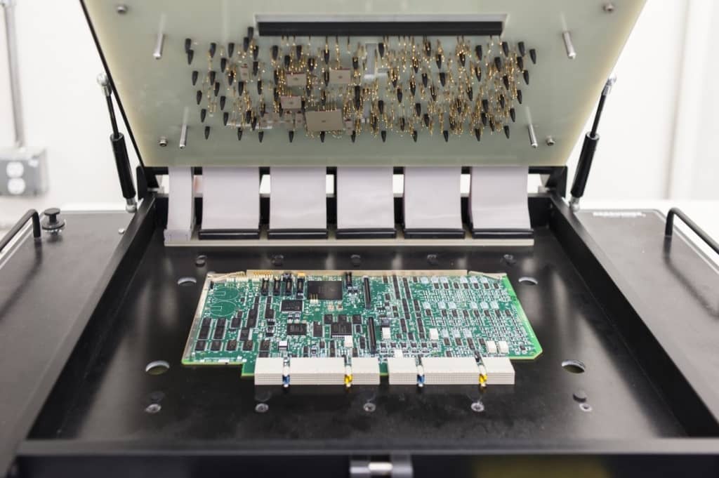
In-Circuit Testing (ICT): A Critical Method for PCB Integrity
- Detects electrical failures
- Verifies component functionality
- Essential for high-volume production
Flying Probe Testing: Best for Low-to-Medium Volume Production
- Ideal for prototypes and low-volume production
- Non-invasive and quick
- Can be adapted to complex designs
Automated Optical Inspection (AOI): Essential for High-Speed Quality Control
- Automates visual inspection
- Detects surface defects
- Ideal for high-speed production
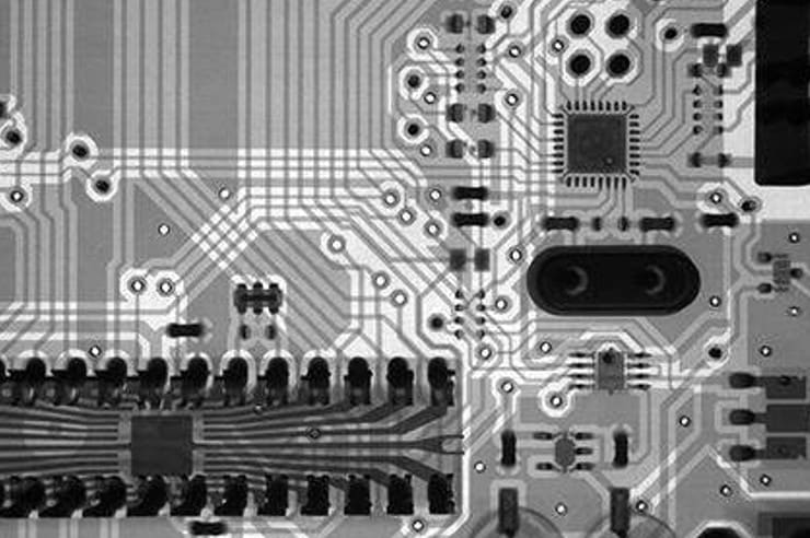
X-Ray Inspection (AXI): Uncovering Hidden Defects in Multilayer PCBs
- Detects hidden defects
- Ideal for multilayer PCBs
- Ensures solder joint integrity
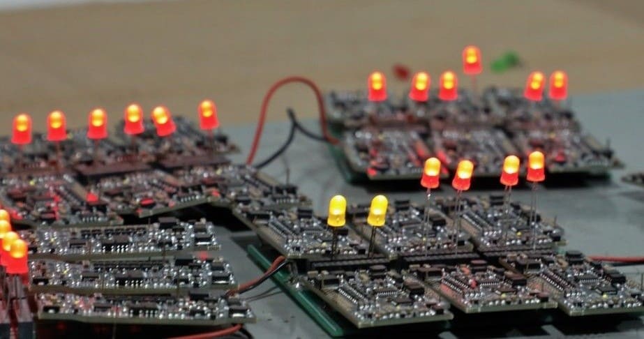
Functional Testing: Ensuring Your PCB Works as Intended
- Tests the PCB under actual working conditions
- Verifies final product performance
- Essential for critical applications
Burn-In Testing: Stress Testing for Long-Term Reliability
- Simulates long-term usage in a short time
- Detects early failures in components
- Improves reliability of final products
Visual Inspection: Identifying Common PCB Defects
Visual inspection remains a fundamental step in the PCB inspection process, especially for identifying common defects like solder joint issues, misaligned components, or visible cracks. A comprehensive PCB visual inspection checklist, combined with the use of an inspection microscope, can significantly improve detection rates. For manual processes, operators often rely on PCB visual inspection standards to ensure consistent and reliable results.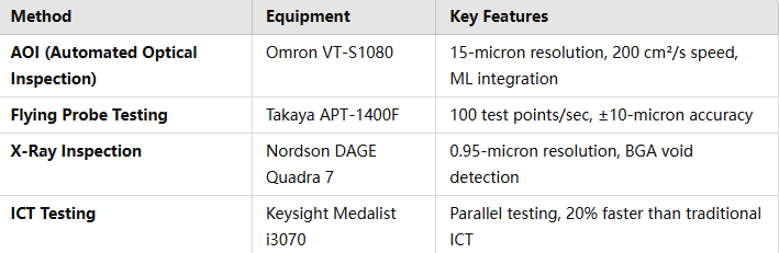
Solderability Testing: Ensuring Robust Solder Joints for Durability
- Checks solderability of components
- Ensures robust and durable solder joints
- Prevents soldering defects such as cold joints
Best Practices for PCB Quality Assurance
Implement Multistage Inspections
Implement Multistage Inspections: Ensure that multiple PCB inspection methods, such as PCB manual visual inspection, ICT testing, and automated optical inspection, are applied at various stages of the PCB production process. Using the right PCB inspection tools and adhering to industry PCB inspection standards can help detect and resolve issues early, ensuring consistent quality throughout production.Maintain Accurate Documentation
Keep thorough records of each inspection and test conducted. This will help in identifying trends in defects and in improving future production runs.Use Automated Systems Where Possible
Automation speeds up the inspection process, improves accuracy, and reduces human error, especially for high-volume productions.Regularly Calibrate Equipment
Calibration ensures that your inspection systems, such as AOI and ICT machines, are working at peak efficiency and providing accurate results.
PCB inspection methods such as AOI, ICT, and X-Ray Inspection are not only critical for defect detection but also essential for meeting global quality standards. Standards like IPC-A-610 and ISO 9001 ensure that your PCBs meet the highest industry benchmarks for reliability, safety, and performance. For instance, IPC-A-610 is widely recognized as the authoritative standard for electronics assembly acceptability, while ISO 9001 focuses on maintaining quality management systems throughout the manufacturing process. By aligning your inspection process with these standards, you can reduce defect rates, enhance customer satisfaction, and build trust with end-users.
Frequently Asked Questions
Choosing the right inspection method depends on:
- Production Volume: Use flying probe testing for prototypes or small batches, and ICT or AOI for high-volume production.
- Product Complexity: High-density or multilayer PCBs benefit from combining AOI and X-Ray inspection.
- Industry Needs: Critical sectors (e.g., medical, aerospace) require functional and burn-in testing for reliability.
- Budget: Flying probe is cost-effective for small runs, while AOI and ICT are ideal for larger scales.
Need help deciding? Contact us for expert advice.
Automated Optical Inspection (AOI) is essential in PCB production for:
- Quick defect detection: Identifies solder misalignment, shorts, and missing components during the PCB inspection process.
- Improved efficiency: AOI is faster and more precise than manual checks, making it ideal for printed circuit board testing.
- 3D Capabilities: Advanced pcb automated optical inspection machines can check solder joint height and volume for compliance with IPC-A-610 standards.
AOI is a critical tool in ensuring high-quality PCB inspection methods.
Both flying probe testing and ICT (In-Circuit Testing) are essential in pcba testing, but they differ in their applications:
- Flying Probe Testing:
- Best for prototypes or small-batch production.
- No need for a custom pcb testing fixture, making it cost-effective.
- Tests individual PCB test points for connectivity and shorts.
- ICT Testing:
- Ideal for high-volume production.
- Requires a custom pcb testing kit or fixture for faster testing.
- More efficient for large-scale manufacturing.
Choose based on production volume and cost considerations.
To ensure compliance with IPC-A-610 standards, follow these steps:
- Use Automated Tools: Implement advanced PCB inspection tools, like AOI and X-Ray systems, to meet quality benchmarks.
- Follow a Checklist: Develop a detailed PCB visual inspection checklist to guide manual and automated inspections.
- Adopt Standards: Align your processes with pcb visual inspection standards and protocols.
- Train Your Team: Ensure your team is skilled in visual inspection and familiar with quality requirements.
Compliance ensures your PCBs meet industry standards, reducing defects and improving customer satisfaction.
Conclusion
👉 See how our Turnkey PCB Assembly can help »
Limited Time Offer:
Get $100 off your order TODAY!
 Trusted by 100+ businesses worldwide No hidden fees – transparent pricing Guaranteed quality with on-time deliver
How PCB Inspection Methods Improve Real-World Applications
PCB inspection methods are widely used across industries to improve production efficiency and product reliability. Here are some real-world examples:
- Consumer Electronics: A smartphone manufacturer reduced defective PCBs by 40% by implementing AOI and X-Ray inspection in the SMT process.
- Aerospace: A leading aerospace company ensured compliance with AS9100 standards by combining ICT testing and flying probe testing for high-reliability PCB assemblies.
- Medical Devices: Functional testing helped a medical device manufacturer achieve a 98% yield rate for their PCBs used in MRI machines, ensuring strict compliance with FDA regulations.
Request for Quote
RECENT POSTS
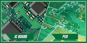
IC Boards Explained: Applications, Layout Tips, and Assembly Services
Discover what IC boards are, how they’re used in modern electronics, and how to design
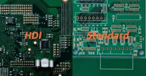
HDI PCB vs Multilayer PCB: How to Choose the Right One for Cost, Signal Integrity & Manufacturing
HDI PCB vs multilayer PCB explained from a manufacturing and assembly perspective. Learn how cost,
RELATED POSTS
Leading PCBA Manufacturer
✅ Assemble 20 PCBAS for $0 ✅ Get $100 OFF – Risk-Free Trial!
✅ 100+ Satisfied Customers
✅ Ensured Quality & On-Time Delivery
✅ Free Trial, No Commitments!