Quick Leads
Transistor Pin Layout – Complete Guide for PCB Assembly & Component Sourcing
Transistors are essential components in modern electronics, serving as both amplifiers and switches in countless applications.
Understanding the transistor pin layout—the exact arrangement and function of each terminal—is critical for ensuring proper integration into PCB designs. Incorrect pin configurations can lead to circuit failure, costly rework, and delayed product delivery.
This complete guide will not only explain transistor pin configurations and their variations, but also provide real PCB assembly examples from our production lines. Whether you are an engineer designing a prototype, a buyer sourcing components for mass production, or a student learning electronics, you’ll find practical tips to ensure accurate layouts and smoother manufacturing.
What Are Transistor Pinouts?
A transistor pin layout (also known as a transistor pinout or transistor pin diagram) refers to the physical arrangement and labeling of a transistor’s terminals. These pins are critical to the device’s function and determine how it connects to the rest of the circuit.
The most common types of transistors include:
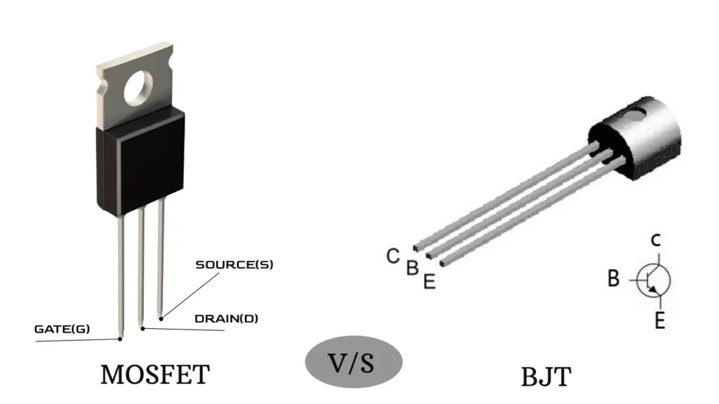
BJTs – Base (B), Collector (C), and Emitter (E)
MOSFETs – Gate (G), Drain (D), and Source (S)
Understanding the correct pin configuration is essential to avoid reverse connections, circuit malfunction, or even component damage.
For PCB Assembly Buyers: When preparing your Gerber and BOM files, always include detailed pin layout diagrams. This ensures accurate component placement, faster assembly, and fewer costly reworks.
Unit Circuits: Leading PCBA Manufacturer
 ISO-certified & 8+ years of PCBA
 Low MOQ & Fast Turnaround
 Prototype & Mass production
Limited Time Offer:
Get $100 off your order TODAY!
Common Transistor Types and Their Pin Configurations
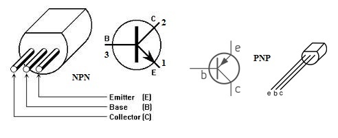
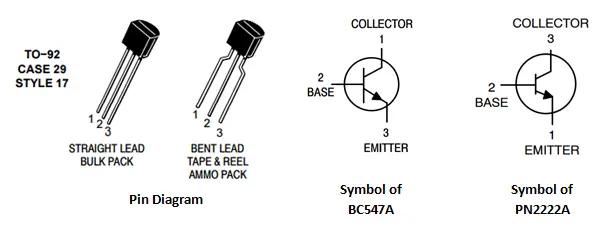
NPN Transistor
- Pinout: Base (B), Collector (C), Emitter (E).
- Diagram:
 C
\
B
/
E
Typical Use Case:
NPN transistors are widely used in digital switching applications. For example, they can turn an LED or relay on and off in response to a microcontroller’s signal. In industrial PCB assemblies, NPN transistors are often part of control circuits for motors, sensors, or safety interlocks.PCB Assembly Insight: When ordering PCBA services, ensure the NPN transistor orientation is clearly marked in your assembly drawings. This prevents reversed installation during mass production, which can cause component failure and costly rework.
PNP Transistor
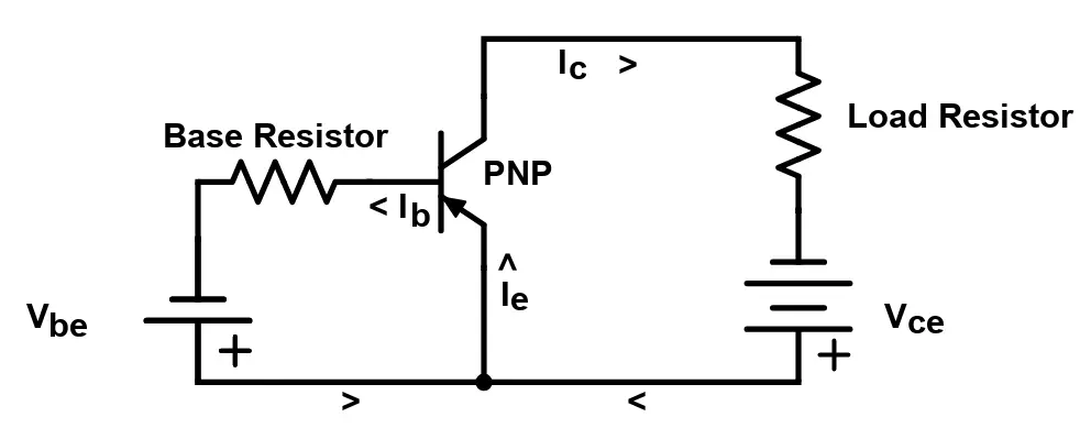
Pinout: Base (B), Collector (C), Emitter (E).
Key Difference from NPN:
In a PNP transistor pin configuration, the current flows from the emitter (E) to the collector (C), which is the opposite direction of an NPN transistor. This polarity difference is critical when designing PCB layouts or troubleshooting circuits.Typical Use Case:
PNP transistors are commonly used in high-side switching, where the load is connected to the ground and the transistor controls the positive voltage. In industrial PCBA projects, they are often applied in safety circuits, power management boards, and sensor control systems.PCB Assembly Insight: Always verify the transistor orientation and pin layout with the manufacturer’s datasheet before mass production. Misplacing a PNP transistor can cause short circuits and delay delivery schedules.
MOSFET (N-Channel and P-Channel)
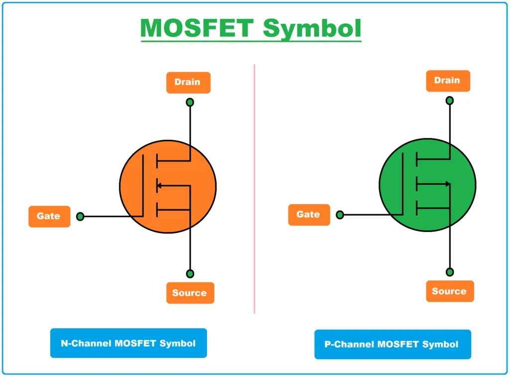
Pinout: Gate (G), Drain (D), Source (S).
Key Differences:
N-Channel MOSFET: Conducts when a positive voltage is applied to the gate relative to the source.
P-Channel MOSFET: Conducts when a negative voltage is applied to the gate relative to the source.
Typical Use Cases:
MOSFETs are ideal for switching and amplifying high-current loads. In industrial PCB assemblies, they are widely used in:Motor control boards
Power supply circuits
Battery management systems
High-efficiency LED drivers
PCB Assembly Insight: Always specify whether an N-Channel or P-Channel MOSFET is required in your BOM and assembly drawings. The wrong selection or incorrect pin orientation can result in overheating, power loss, or complete circuit failure.
JFET
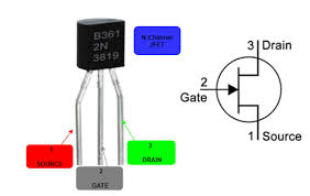
Pinout: Gate (G), Source (S), Drain (D).
Unique Feature: Operates without the insulation layer found in MOSFETs.
Darlington Transistor
Pinout: Similar to BJTs, with two internally connected transistors for high gain.
Use Case: Amplification in low-signal circuits.
How to Identify NPN vs. PNP Transistors
Correctly identifying a transistor type is essential for ensuring the transistor pin layout is connected properly during PCB assembly. Here are two reliable methods:
1. Using Circuit Symbols
-
NPN Transistor Symbol: The emitter arrow points outward.
-
PNP Transistor Symbol: The emitter arrow points inward.
(ALT text suggestion for image: “NPN vs PNP transistor circuit symbols – emitter arrow direction”)
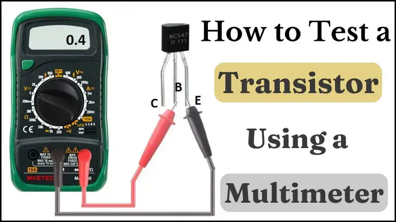
2. Using a Multimeter (Diode Mode)
-
Set the multimeter to diode mode.
-
Test the current flow between terminals:
-
Positive probe to base: Current flows for NPN, but not for PNP.
-
Negative probe to base: Current flows for PNP, but not for NPN.
-
PCB Assembly Insight: Even if the schematic is correct, misidentifying NPN and PNP transistors during production can result in reversed installation, leading to defective boards. At UnitCircuits, we verify transistor pin configurations during component inspection to prevent such errors in mass production.
Applications&Troubleshooting Tips
Common Applications in PCB Assembly
-
Switching: Control LEDs, relays, motors, and solenoids in both consumer electronics and industrial automation systems.
-
Amplification: Boost weak audio, RF, or sensor signals in communication devices, instrumentation, and safety monitoring systems.
-
Logic Gates: Implement digital logic functions in computing, robotics, and intelligent control equipment.
In large-scale PCB manufacturing, choosing the correct transistor pin configuration is essential to avoid costly rework and delays.
Troubleshooting Transistor Pin Layouts
-
Use the Manufacturer’s Datasheet
-
Verify the exact pin configuration for the specific package type (TO-92, SOT-23, etc.).
-
-
Test with a Multimeter
-
In diode mode, confirm correct current flow and polarity before soldering.
-
-
Check Orientation Before Assembly
-
Misaligned pins can cause overheating, short circuits, or complete device failure.
-
-
Prevent Overload
-
Ensure the transistor’s maximum voltage and current ratings are not exceeded in your design.
-
PCB Assembly Insight: At UnitCircuits, we run component orientation checks and functional testing to ensure every transistor is placed correctly before mass production. This minimizes returns, improves reliability, and speeds up delivery schedules.
For more information, visit below:
Frequently Asked Questions (FAQs)
To read a pinout diagram, first identify the transistor’s type (e.g., NPN, PNP, MOSFET). Then match the labeled pins (e.g., Base, Collector, Emitter) to the physical terminals on the transistor. Datasheets often provide orientation guides, such as top-down or side views, to help you identify each terminal.
Misconnecting a transistor’s pins can lead to overheating, circuit failure, or permanent damage to the component. It may also cause incorrect operation, such as a switch not turning on or an amplifier not amplifying. Always verify the pin configuration before connecting the transistor.
You can identify the type by:
- Datasheet: Check the manufacturer’s datasheet for explicit information.
- Symbol: Look for the direction of the emitter arrow in the circuit symbol (outward for NPN, inward for PNP).
- Multimeter Test: In diode mode, measure the current flow between the Base and other terminals. Current flows from Base to Emitter in NPN and from Emitter to Base in PNP.
A multimeter in diode mode is the most common tool for identifying transistor pinouts. Additionally:
- Refer to the transistor’s datasheet for precise pin configurations.
- Use an SMD codebook for Surface-Mount Device (SMD) transistors.
- Online resources like transistor databases can help with older or less common models.
No, simply matching the pinout does not ensure compatibility. You must also check the transistor’s:
- Voltage and Current Ratings: Ensure it can handle the required power.
- Gain (hFE): The amplification factor must be suitable for your circuit.
- Frequency Characteristics: Some applications, like RF circuits, require specific transistor properties. Always cross-check the datasheet to confirm suitability.
Limited Time Offer:
Get $100 off your order TODAY!
 Trusted by 100+ businesses worldwide
 No hidden fees – transparent pricing
 Guaranteed quality with on-time deliver
Conclusion
Understanding transistor pinouts is fundamental to successful circuit design. Always start with datasheets, test with a multimeter, and practice with simple circuits. With these tips and tools, you’ll be ready to integrate transistors into your projects confidently.
Key Takeaways:
Definition of Transistor Pinouts:
- Transistor pinouts refer to the arrangement of its terminals, which vary based on the type of transistor (e.g., NPN, PNP, MOSFET).
Importance of Pinouts:
- Understanding pinouts is essential for correct circuit integration, preventing malfunctions, and ensuring optimal performance.
Common Transistor Types:
- BJTs (NPN and PNP): Use Base, Collector, and Emitter terminals.
- MOSFETs (N-Channel and P-Channel): Use Gate, Drain, and Source terminals.
- JFETs and Darlington transistors have unique pin configurations suited for specific applications.
Identification Tips:
- Use datasheets, multimeters, or circuit symbols to identify transistor types (e.g., NPN vs. PNP).
Applications:
- Transistors are widely used as switches, amplifiers, and logic gates in electronics.
Request for Quote
RECENT POSTS
Multilayer PCB Signal Integrity: Expert Design Rules for Noise-Free Performance
Discover expert multilayer PCB signal integrity design rules and turnkey assembly solutions to ensure noise-free,
What is HDI PCB? | Ultimate Guide to Benefits, Structure, and Real-World Applications
Discover what HDI PCB is, how it works, and why our turnkey HDI PCB assembly
RELATED POSTS
Leading PCBA Manufacturer
✅ Assemble 20 PCBAS for $0 ✅ Get $100 OFF – Risk-Free Trial!
✅ 100+ Satisfied Customers
✅ Ensured Quality & On-Time Delivery
✅ Free Trial, No Commitments!
