Quick Leads
Understanding Ball Grid Array (BGA) Technology in PCB Design | Comprehensive Guide
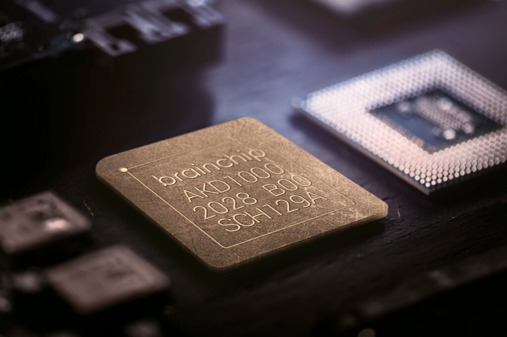
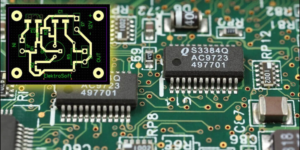
What is a Ball Grid Array (BGA) on a PCB?
History of BGA Technology
Advantages of BGA in PCB Design
- Higher Density Connections: BGA allows for more connections in a smaller space, which is important for small devices.
- Enhanced Thermal Performance: The solder balls in BGA packages help dissipate heat, which is important for high-performance components.
- Superior Electrical Performance: BGA’s shorter electrical paths reduce inductance and resistance, which improves signal integrity.
How BGA Compares to QFP and CSP in PCB Design
- QFP Packaging: QFPs have external leads that can bend, which limits their use in high-density applications. They also have fewer connections compared to BGA.
- CSP Packaging: CSPs are smaller than BGAs, so they work well in space-constrained applications. However, they are usually more expensive and can be more difficult to manufacture.
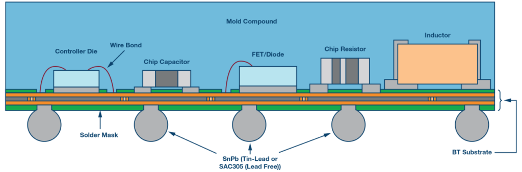
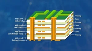
The BGA Manufacturing and Assembly Process
- Stencil Printing: Applying solder paste to the PCB pads where the BGA will be placed.
- Component Placement: Accurately positioning the BGA on the PCB, aligning the solder balls with the corresponding pads.
- Reflow Soldering: Heating the assembly in a reflow oven to melt the solder balls, creating robust electrical connections.
Challenges and Solutions in BGA Technology
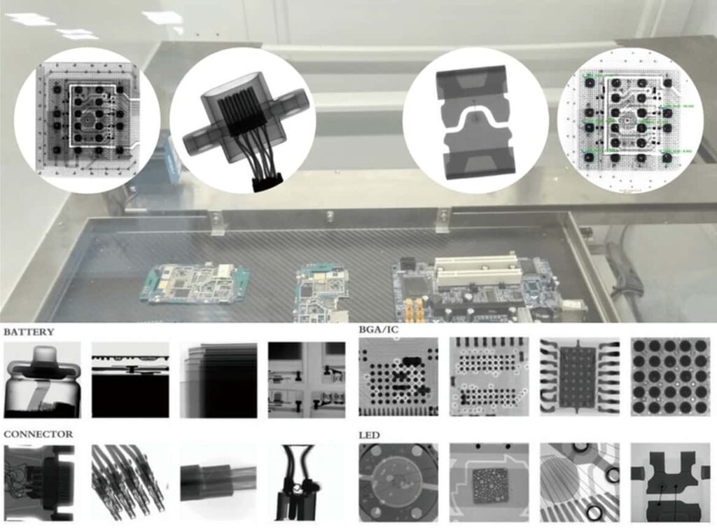
- Solder Joint Inspection:Traditional visual inspection methods don’t work because you can’t see the solder joints under the package. You need advanced inspection techniques like X-ray.
- Rework Difficulty:Reworking a BGA is difficult and risky because you can damage nearby components. It’s important to get it right the first time to avoid expensive rework.
How to Inspect BGA Solder Joints
- X-ray Inspection:X-ray imaging can see through the BGA package and show you defects like voids or cold joints that you can’t see with traditional methods.
- Automated Optical Inspection (AOI): You can modify AOI systems to check the alignment of solder balls before reflow. This helps you catch misalignments early in the process.
Applications of BGA Technology in High-Performance Electronics
- CPUs and GPUs: These processors require the dense interconnections and thermal efficiency provided by BGA.
- Mobile Devices: BGAs’ compact size makes them ideal for smartphones, tablets, and wearables.
- Networking Equipment: Routers, switches, and other networking devices benefit from BGA’s ability to handle high-speed signals and large data volumes.
Future Trends in BGA Technology
- Micro BGAs: These smaller BGA packages offer finer pitch, supporting further device miniaturization.
- Impact of 5G and IoT: The demands of 5G and IoT devices are driving the development of BGAs capable of handling higher frequencies and data rates.
- Lead-Free BGAs: Environmental regulations are pushing for the use of lead-free solder balls, which present new challenges in reliability and manufacturability.
Limited Time Offer:
Get $100 off your order TODAY!
 Trusted by 100+ businesses worldwide No hidden fees – transparent pricing Guaranteed quality with on-time deliver
Frequently Asked Questions
Both BGA (Ball Grid Array) and QFN (Quad Flat No-Lead) packages have their advantages depending on what you’re trying to do. BGA is better for high-density connections and better thermal performance, so it’s great for high-performance devices like CPUs and GPUs. QFN packages, on the other hand, are better for low-profile, cost-sensitive applications where you don’t need a lot of pins.
Yes, you can rework a BGA, but it’s a complicated and delicate process. To rework a BGA, you have to remove the bad chip, clean the pads on the board, put new solder paste on the pads, and then reflow a new BGA package onto the board. Because you can’t see the solder joints, you have to be really precise, and you usually need specialized equipment like rework stations with infrared heating and X-ray inspection.
Common defects in BGA solder joints include voids, cold joints, misalignment, and insufficient solder. These defects can cause problems with the electrical and mechanical connection, which can lead to device failure. You usually need advanced inspection methods like X-ray and Automated Optical Inspection (AOI) to find these problems.
BGA makes electronic devices work better by allowing for more connections in a smaller space, better heat dissipation, and shorter electrical paths. These things help you have better signal integrity, faster processing speeds, and more reliability. That’s really important for high-performance applications like CPUs, GPUs, and advanced networking equipment.
BGA (Ball Grid Array) and CSP (Chip Scale Package) are both types of surface-mount packaging, but CSP is generally smaller and more compact than BGA. CSP packages are closer in size to the actual chip, so they work well in really small devices. BGA, on the other hand, has better thermal and electrical performance because it’s bigger and has a more robust connection system. That’s why you see BGA in high-performance applications.
Ensuring the reliability of BGA solder joints involves good design, good manufacturing, and good inspection. Using advanced X-ray inspection to detect defects, making sure you have precise reflow soldering temperatures, and using the right solder paste all contribute to making good connections. Also, ongoing testing and quality control measures help keep BGA assemblies working well over time.
Summary
Call to Action (CTA)
Request for Quote
RECENT POSTS
Multilayer PCB Signal Integrity: Expert Design Rules for Noise-Free Performance
Discover expert multilayer PCB signal integrity design rules and turnkey assembly solutions to ensure noise-free,
What is HDI PCB? | Ultimate Guide to Benefits, Structure, and Real-World Applications
Discover what HDI PCB is, how it works, and why our turnkey HDI PCB assembly
RELATED POSTS
Leading PCBA Manufacturer
✅ Assemble 20 PCBAS for $0 ✅ Get $100 OFF – Risk-Free Trial!
✅ 100+ Satisfied Customers
✅ Ensured Quality & On-Time Delivery
✅ Free Trial, No Commitments!