Quick Leads-PCBA
 Looking for full-service PCB Assembly?
Turnkey solutions from PCB manufacturing to testing.
sales@unitcircuits.com
🟢Why 2-Layer PCBs Still Matter in a Multi-Layer World
Let’s be honest: most of the buzz in PCB design today is about HDI, flex-rigid stacks, and 8+ layer boards. But in the real world, especially for cost-sensitive, compact, and low-to-mid complexity devices, 2 layer PCBs still dominate.
And for good reason. They’re simple, affordable, and — when done right — more than capable of powering the next great IoT device, sensor node, LED driver, or embedded controller.
In this guide, I’ll break down:
-
What a 2-layer printed circuit board is
-
How it compares to other stackups
-
Smart layout and manufacturing strategies
-
Real pain points we solve daily with better assembly workflows
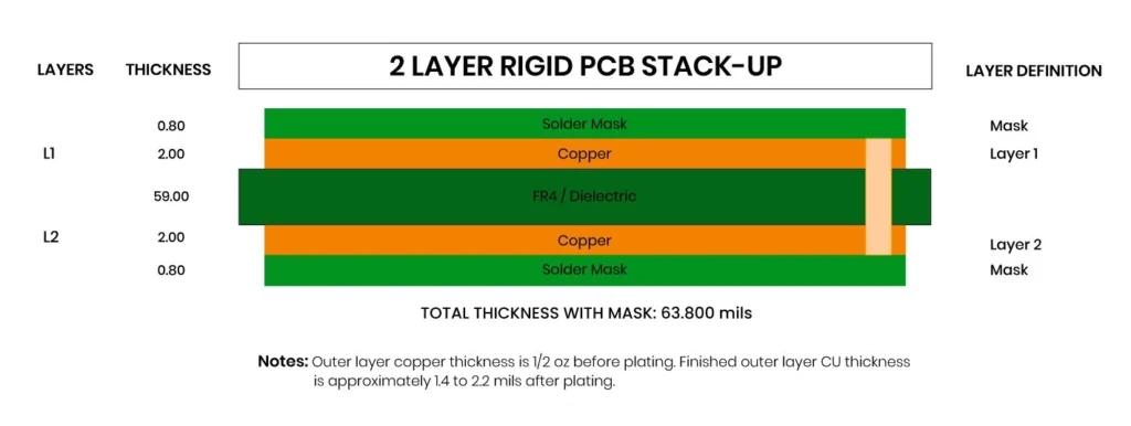
📌 What Is a 2 Layer PCB?
A 2-layer PCB (also called a double-layer PCB or two-layer PCB board) is a printed circuit board with two conductive copper layers: one on the top side and one on the bottom.A 2-layer PCB is an excellent middle-ground for compact electronics, combining cost-efficiency with moderate routing capability. Learn more about the basic structure and use cases of 2-layer PCBs.
Unlike single-layer boards, these use vias to interconnect traces between the two sides. This allows more complex routing and component placement while staying cost-effective.
These boards are built from:
Base substrate (usually FR4)
Top and bottom copper layers
Solder mask (for insulation)
Silkscreen (for labeling)
While a 2-layer PCB defines the physical structure of the board, it’s important to understand how it fits into the broader manufacturing process. In real production, most double-layer boards are delivered as complete PCBA solutions, where components are mounted, soldered, and tested. If you’re new to this distinction, this guide on what PCBA is and how it differs from a bare PCB explains how design decisions directly affect assembly cost, yield, and reliability.
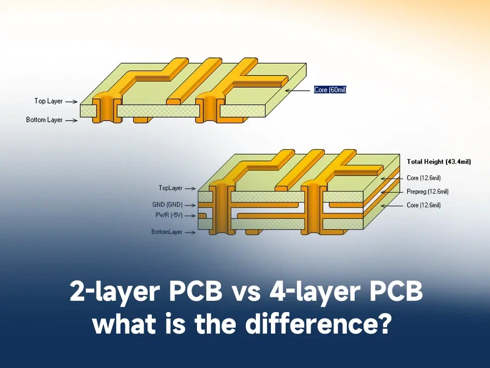
🔍 Double Layer PCB vs 4-Layer: A Quick Cost & Use Case Breakdown
📊 Comparison Chart:
| Feature | 2-Layer PCB | 4-Layer PCB |
|---|---|---|
| Cost per board | Lower (budget-friendly) | Higher (due to added layers) |
| Turnaround time | Faster (simple stackup) | Slightly longer |
| Signal routing | Moderate | Excellent for complex signals |
| EMI performance | Basic | Superior (dedicated ground/power) |
| Best for | IoT, LED drivers, consumer gear | RF, high-speed, dense computing |
When balancing price and performance, understanding the cost differences between 2-layer and multi-layer PCBs can help you make the right design choice early on.
🧱 Structure of a 2-Layer Printed Circuit Board
🧩 Top & Bottom Layers
Each side of a 2-layer PCB has copper traces, meaning more design flexibility than a 1-layer board. You can route signals on one side and use the other for ground or power, or split them functionally.
🔩 Through-Hole Vias
Copper-plated vias connect top and bottom layers. This is where 2 layer PCB stackup differs most from multi-layer designs — you don’t get buried or blind vias, only through-hole.
🧱 Materials
The most common material for 2 layer PCBs is FR4, known for:
Good strength-to-cost ratio
Moderate thermal resistance (TG ~135–180°C)
Acceptable for most consumer and industrial applications
Other materials include:
Polyimide (for higher-temp or flex-rigid boards)
CEM-1 (lower-cost option for basic applications)
🧠 Advantages of 2 Layer PCBs
✅ 1. Cost-Effective Manufacturing
A major advantage of 2 layer PCBs is their low fabrication and assembly cost. That’s especially important when launching new products, prototyping, or building low-volume runs.
Our clients often choose low cost 2 layer PCB fabrication to validate designs before scaling up.
✅ 2. Faster Turnaround
Less complexity means:
Shorter fab lead times
Fewer setup requirements for assembly
Easier testing and DFM checks
If you need a prototype 2 layer PCB in 3–5 days, we’ve got you covered.
✅ 3. Great for Compact Electronics
Think about:
Smart door sensors
Thermostats
Handheld remotes
Power modules
These all run perfectly on 2 layer PCBs for IoT devices or consumer gadgets, especially when combined with good SMT assembly.
Unit Circuits: Leading PCBA Manufacturer
 ISO-certified & 8+ years of PCBA Low MOQ & Fast Turnaround Prototype & Mass production
Limited Time Offer:
Get $100 off your order TODAY!
sales@unitcircuits.com
🛠️ How to Design a 2 Layer PCB (The Smart Way)
Designing a 2-layer board doesn’t mean cutting corners — it just means designing smarter.
Here are some layout tips we swear by:
📌 Use One Layer as Ground
For most 2 layer PCB layouts, use the bottom layer as a dedicated ground plane. This improves:
Signal integrity
Return path efficiency
EMC behavior
📌 Route Signals Strategically
Stick to:
Shorter traces
Clear separation between analog and digital signals
Power traces with sufficient width (based on current)
💡 Don’t forget to calculate trace width and spacing — especially for high-current paths.
📌 Minimize Via Count
Vias cost money and space. Use them only when needed.Following practical layout tips for 2-layer PCBs can help reduce EMI and improve power distribution — even in dense designs.
📐 Recommended Design Parameters
📊 2 Layer PCB Design Rules Chart
| Design Element | Recommended Value |
|---|---|
| Minimum Trace Width | 6 mil (0.15 mm) |
| Minimum Trace Spacing | 6 mil |
| Via Drill Size | 0.3 mm |
| Copper Weight | 1 oz (standard) |
| Annular Ring Size | ≥0.15 mm |
| Min Pad Size for ICs | Based on IPC-7351 standards |
🔄 2 Layer PCB Manufacturing Process
Knowing how your board is made helps with better DFM.
🔧 Step-by-Step Overview
Design files prepared (Gerber, BOM, drill, pick-and-place)
Laminated base prepared with top and bottom copper
Copper etching forms traces
Drilling vias and through-holes
Plating vias with copper
Solder mask + silkscreen printing
Surface finish (HASL, ENIG, etc.)
Electrical testing
SMT or THT assembly
🔍 SMT Assembly for 2 Layer PCB
We often use SMT assembly for 2 layer PCBs when compact size and fast production matter. Benefits include:
Precision IC placement
Faster soldering
Lower labor cost
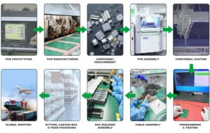
We also handle THT for connectors, relays, or power components, giving you full flexibility.From a manufacturing perspective, even a simple 2-layer PCB goes through a well-defined assembly workflow. Steps such as solder paste printing, SMT placement, reflow soldering, inspection, and testing all influence final board quality. This overview of the essential steps in PCB assembly helps designers understand where common defects originate—and how good DFM practices can prevent costly rework on double-layer boards.
Most modern 2-layer PCBs rely heavily on surface-mount assembly to achieve compact layouts and lower production costs. However, connectors, relays, or power components may still require through-hole processes. Understanding the differences between SMT, SMD, and THT assembly techniques helps engineers choose the right combination for performance, reliability, and manufacturability—especially when designing mixed-technology double-layer boards.
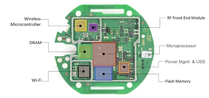
🧩 Applications of 2 Layer PCBs in Electronics
Here are just a few popular use cases we help build daily:
🧠 Embedded Systems
Microcontrollers, EEPROM, temperature sensors
🌐 IoT Devices
LoRa nodes, WiFi controllers, BLE sensors
→ 2 layer PCB for IoT devices is often enough unless RF constraints apply
🔋 Power Supplies
Basic SMPS, LED drivers, low-voltage converters
💡 Lighting & Control Boards
2-layer is ideal for single-color LED panels or relay modules
🚧 Common Pain Points (And How We Solve Them)
❌ Problem 1: Overcomplicating Design for Simple Boards
Some engineers over-design — using 4-layer boards when 2-layer works just fine.
✅ Our Tip: We help validate your stackup and optimize layout before production — saving you $$$.
❌ Problem 2: EMI & Signal Issues in Dense 2-Layer Layouts
No dedicated plane = potential interference or noise issues
✅ Our Solution: We provide layout guidance, especially for 2 layer PCB ground plane optimization.
❌ Problem 3: Poor DFM Practices
Unconnected pads, overlapping silkscreen, bad via placement…
✅ Our Solution: Free DFM review + stencil optimization included in every quote.
❌ Problem 4: Assembly Failures Due to Tight Pitch SMT Parts
Small-pitch QFNs, misaligned passive components
✅ Our SMT Line: 0201 support, paste inspection, and X-ray for QFNs or BGAs (if used)
🌎 Sourcing a Reliable 2 Layer PCB Manufacturer in China
Here’s what to check:
✅ SMT & THT Capability
Can they handle both for a two-layer PCB board with mixed components?
✅ Support for Prototyping
We offer low volume 2 layer PCB production with no setup fee.
✅ Full-Service Assembly
We cover everything: fab, sourcing, SMT, QA — you just send us the files.
FAQs
1. What is a two layer PCB used for in real-world applications?
A two layer PCB is commonly used in IoT devices, consumer electronics, lighting systems, and power modules where moderate complexity and compact design are required. It provides enough routing flexibility for microcontrollers, sensors, and connectors while keeping costs low — making it ideal for prototyping and small-batch production.
2. How to design a 2 layer PCB with minimal EMI issues?
design a 2 layer PCB with minimal EMI, dedicate one layer to ground, avoid routing high-speed signals near analog paths, and use proper decoupling capacitors. Keeping return paths short and using consistent trace widths also helps improve electromagnetic performance, especially in compact double-layer PCB designs.
3. What is the difference between 2 layer PCB and 4 layer PCB in signal integrity?
A 2 layer PCB offers basic signal integrity with limited layer separation, while a 4 layer PCB provides dedicated power and ground planes that significantly reduce noise and crosstalk. If your design requires high-speed signals or controlled impedance, a 4-layer PCB is the better option.
4. What is the key advantage of double-layer PCBs in low-volume manufacturing?
Double-layer PCBs are cost-effective for low-volume manufacturing because of simpler stackups, faster turnaround times, and reduced fabrication complexity. If you're developing a small batch or MVP (minimum viable product), a 2 layer PCB balances price and performance without over-engineering your design.
Have Specific Requirements?
Looking for high-precision PCB assembly for your products? Our team specializes in delivering top-tier assembly services, ensuring your devices perform flawlessly in any environment. Contact us today for a free consultation on how we can enhance your product’s reliability.
🧾 Conclusion: Build Smarter with 2 Layer PCBs
Here’s the truth: you don’t always need a 6-layer board with buried vias to build a great product. For many applications, a well-designed 2 layer PCB is the perfect balance of performance, cost, and manufacturability.
At Unit Circuits, we help engineers and startups go from schematic to shipment without the typical manufacturing headaches.
📨 Need a quote or just want to validate your 2-layer design? Contact us for a free review — and we’ll help you build better, faster, and more affordably.
Save on your next PCB project?
Claim $100 OFF your order today.
sales@unitcircuits.com
✅ high-quality PCB assembly with strict quality control ✅ ISO-certified & 8+ years of experience. ✅ Low MOQ, fast turnaround, and 100% E-tested PCBs.
Additional Resources:
- How to Repair Circuit Boards: A Step-by-Step Beginner’s Guide
- Capacitor on Circuit Board: A Comprehensive Guide
- What Are PCB Conformal Coatings? Types, Benefits, and Applications Explained
- SMD Size Codes Explained: A Complete Guide to Understanding Surface-Mount Component Dimensions
- AC vs DC: Key Differences, Applications, and Advantages in Modern Electronics
Request for Quote
sales@unitcircuits.com
RECENT POSTS
IC Boards Explained: Applications, Layout Tips, and Assembly Services
Discover what IC boards are, how they’re used in modern electronics, and how to design
HDI PCB vs Multilayer PCB: How to Choose the Right One for Cost, Signal Integrity & Manufacturing
HDI PCB vs multilayer PCB explained from a manufacturing and assembly perspective. Learn how cost,
RELATED POSTS

Leading PCBA Manufacturer
✅ Assemble 20 PCBAS for $0 ✅ Get $100 OFF – Risk-Free Trial!
sales@unitcircuits.com
✅ 100+ Satisfied Customers
✅ Ensured Quality & On-Time Delivery
✅ Free Trial, No Commitments!