Quick Leads-PCBA
Introduction: Why PCBs Matter for 5G & IoT Success
Imagine a smart home device suddenly losing connectivity—a thermostat failing to adjust temperatures, a security system disconnecting, or a smart light lagging. For IoT brands like Shelly USA, these failures can mean product recalls, customer complaints, and revenue loss.
The problem? Outdated PCB technology that can’t handle high-speed 5G signals, miniaturized IoT sensors, and real-world interference.
The solution? Next-generation PCB materials and designs that ensure faster data transmission, better reliability, and lower power consumption—essential for high-volume IoT manufacturing in 2025.
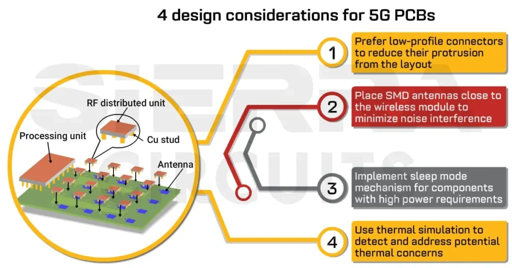
What Makes a PCB “5G & IoT-Ready” in 2025?
✅ Handles high-frequency 5G signals without interference
✅ Minimizes power consumption for long-lasting IoT battery life
✅ Supports miniaturization for compact smart devices
✅ Reduces manufacturing costs for high-volume production
Many IoT brands struggle with these challenges, but the latest advanced PCB solutions are designed to solve them at scale.
Why This Matters for IoT Brands Like Shelly USA
🚨 The Business Problem
Companies like Shelly USA need cost-effective, high-quality PCB assembly for simple but scalable smart home devices.
❌ What’s at Stake?
- Connectivity failures → Customer complaints, bad reviews, lost sales
- High power consumption → Shorter battery life, increased costs
- Manufacturing issues → Delays, expensive redesigns
✅ The Solution: High-Speed, RF-Optimized, HDI PCBs
With better PCB technology, IoT brands get:
✅ Stable wireless communication in home automation networks
✅ Lower energy consumption → Longer battery life
✅ Cost-effective production → Scale up without quality loss
💡 Example: Shelly’s smart thermostatic radiator valve head requires ultra-compact, high-speed PCBs for seamless connectivity—our solutions ensure this with high-frequency laminates and precise microvia technology.
Unit Circuits: Leading PCBA Manufacturer
 ISO-certified & 8+ years of PCBA
 Low MOQ & Fast Turnaround
 Prototype & Mass production
Limited Time Offer:
Get $100 off your order TODAY!
Key PCB Innovations That Power 5G & IoT in 2025
1. High-Speed PCB Materials for 5G Connectivity
🚀 Problem: Traditional PCBs cause signal loss at 5G frequencies (24GHz+).
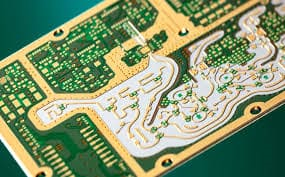
💡 Solution: RF-optimized materials like PTFE, Rogers, and ceramic-filled laminates.
🔹 Why 5G Needs Special PCB Materials
❌ Standard FR4 PCBs lose signal strength at high frequencies.
❌ Poor impedance control causes data corruption.
❌ High temperatures from 5G signals damage PCB performance.
✅ Best PCB Materials for 5G & IoT in 2025:
| Material | Benefits | Best for |
|---|---|---|
| PTFE (Teflon) | Reduces signal loss | 5G base stations, RF antennas |
| Rogers RO4000 Series | High-frequency stability | IoT sensors, wireless devices |
| Hybrid stack-ups (FR4 + RF cores) | Cost-effective & efficient | Mass production of IoT PCBs |
🔹 Use Case: IoT sensors & 5G base stations need these materials for stable, long-range connectivity.
5G PCB design requires specialized materials like PTFE and Rogers to ensure low signal loss and high-frequency stability, as outlined in this 5G PCB research.
2. HDI PCB Technology for Compact IoT Devices
🚀 Problem: IoT devices need small, powerful PCBs, but traditional designs take up too much space.
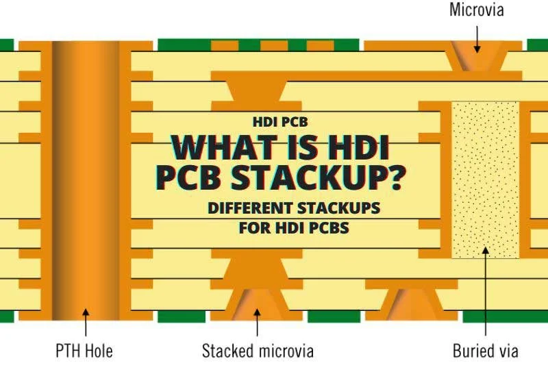
💡 Solution: HDI (High-Density Interconnect) PCBs with microvias & fine-pitch components.
High-Density Interconnect (HDI) PCBs are becoming essential for compact IoT devices, enabling multi-layer miniaturization, as discussed in this HLC PCB article.
🔹 Why HDI PCBs Are Critical for IoT Devices
✔ Microvias & thinner traces → Reduce signal delay
✔ More layers, smaller components → Perfect for compact smart devices
✔ Better heat dissipation → Prevents overheating in high-density circuits
🔹 Use Case: Shelly’s smart radiator valve requires ultra-thin, multi-layer PCBs to fit inside a compact device—HDI technology makes this possible.
3. RF PCB Design: Solving 5G & IoT Interference Issues
🚀 Problem: Interference from other wireless devices can cause dropped signals.
💡 Solution: Better RF shielding, impedance control, and PCB layout.
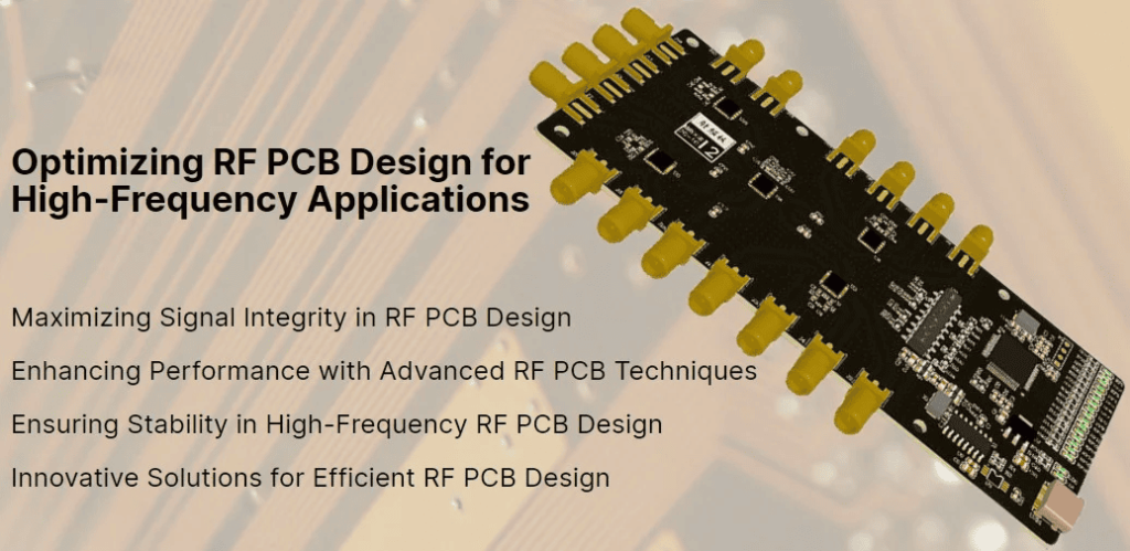
✅ How to Prevent Signal Interference in 5G & IoT PCBs
✔ RF shielding layers → Block external interference
✔ Controlled impedance design → Maintains signal integrity
✔ Optimized PCB stack-ups → Minimizes cross-talk between layers
🔹 Use Case: Smart home IoT hubs & 5G network equipment use these solutions for ultra-stable connections.
To optimize signal integrity in 5G networks, engineers are exploring embedded PCB technologies, as shown in this IEEE study on 5G mmWave PCBs.
Common Challenges in 5G & IoT PCB Manufacturing (and How We Solve Them)
📌 Pain Point 1: Sourcing High-Quality PCB Materials
❌ Many suppliers still use outdated FR4, which fails at high frequencies.
✅ Solution: We source RF-optimized materials like Rogers & Taconic to ensure low-loss PCBs for IoT & 5G applications.
📌 Pain Point 2: Precision Manufacturing for High-Frequency PCBs
❌ High-frequency signals require ultra-precise PCB etching.
✅ Solution: We use laser drilling & LDI (Laser Direct Imaging) for high-accuracy trace routing & microvia formation.
📌 Pain Point 3: Thermal Management in High-Power PCBs
❌ 5G networks generate excessive heat, leading to PCB failure.
✅ Solution: Thermal vias, copper pours & heat spreaders improve heat dissipation.
FAQs
1. How do PCBs affect IoT device battery life?
Poor PCB design leads to high power consumption, draining IoT device batteries faster. Low-power PCB designs, using optimized layouts and power-efficient materials, extend battery life significantly.
2. Can advanced PCBs reduce 5G signal interference?
Yes! RF shielding, proper layer stack-ups, and impedance matching significantly reduce interference, ensuring stable 5G and IoT connectivity.
3. What’s the best PCB material for cost-effective IoT mass production?
A hybrid stack-up (FR4 + high-frequency cores) provides a balance between cost and performance, making it ideal for high-volume IoT manufacturing.
4. Why do some PCBs fail in 5G applications?
Many PCBs can’t handle high-frequency signals, leading to poor signal integrity and data loss. Using PTFE or Rogers materials, along with precision impedance control, ensures reliable 5G performance.
Have Specific Requirements?
Looking for high-precision PCB assembly for your products? Our team specializes in delivering top-tier assembly services, ensuring your devices perform flawlessly in any environment. Contact us today for a free consultation on how we can enhance your product’s reliability.
Final Thoughts: Why the Right PCBs Matter for IoT & 5G Success
The right PCB design makes or breaks a product. For IoT brands, high-quality PCBs ensure reliable connectivity, low power consumption, and cost-effective mass production.
🚀 Need the best PCB solutions for your IoT products?
📌 Let’s build something great together—contact us today!
Save on your next PCB project?
Claim $100 OFF your order today.
✅ high-quality PCB assembly with strict quality control ✅ ISO-certified & 8+ years of experience. ✅ Low MOQ, fast turnaround, and 100% E-tested PCBs.
Additional Resources:
- How to Repair Circuit Boards: A Step-by-Step Beginner’s Guide
- Capacitor on Circuit Board: A Comprehensive Guide
- What Are PCB Conformal Coatings? Types, Benefits, and Applications Explained
- SMD Size Codes Explained: A Complete Guide to Understanding Surface-Mount Component Dimensions
- AC vs DC: Key Differences, Applications, and Advantages in Modern Electronics
Request for Quote
RECENT POSTS
IC Boards Explained: Applications, Layout Tips, and Assembly Services
Discover what IC boards are, how they’re used in modern electronics, and how to design
HDI PCB vs Multilayer PCB: How to Choose the Right One for Cost, Signal Integrity & Manufacturing
HDI PCB vs multilayer PCB explained from a manufacturing and assembly perspective. Learn how cost,
RELATED POSTS
Leading PCBA Manufacturer
✅ Assemble 20 PCBAS for $0 ✅ Get $100 OFF – Risk-Free Trial!
✅ 100+ Satisfied Customers
✅ Ensured Quality & On-Time Delivery
✅ Free Trial, No Commitments!
