Quick Leads-PCBA
HDI PCB design is a game-changer—but it’s not for the faint of heart. Engineers face everything from microvia failure to signal chaos. In this article, I’ll unpack real-world design problems and show you how pros like us solve them—without the fluff.
The most common HDI PCB design problems include routing congestion, via reliability, signal integrity issues, and thermal dissipation. These can be resolved with smart HDI stackup strategies, correct via-in-pad design, precise impedance control, and early collaboration with experienced manufacturers. Tools like IPC-2226 and controlled impedance planning are key to solving these real-world challenges.
Let’s walk through the real problems and practical fixes—plus a few comparisons and visual tips to make things clearer.

🧩 What Is the Difference Between a Standard PCB and an HDI PCB?
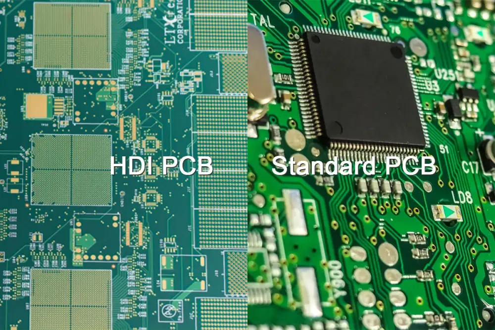
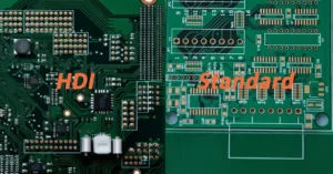
High-Density Interconnect (HDI) PCBs are nothing like your traditional FR4 boards. The key difference lies in how densely components and traces are packed, and how advanced the interconnection methods are.
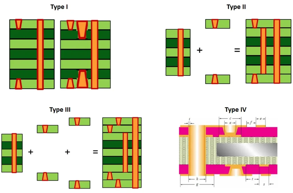
Standard PCBs often rely on through-hole vias and simple layer stacks. In contrast, HDI PCBs use microvias, blind vias, and buried vias, allowing more connections in less space. That’s what makes them perfect for mobile devices, IoT, and high-speed data systems.
📊 Chart 1: Standard PCB vs. HDI PCB
| Feature | Standard PCB | HDI PCB |
|---|---|---|
| Via Type | Through-hole | Microvia, blind/buried |
| Min Trace/Space | ~6 mil | 3 mil or lower |
| Layer Count | 2–8 typical | 8+ with stacked vias |
| Signal Integrity | Basic | Controlled impedance design |
| Cost | Lower | Higher (but scalable) |
| Density | Moderate | Very High |
🚫 What Are the Common HDI PCB Design Mistakes and How to Avoid Them?
Here’s what often goes wrong—and how to get it right.
1. Improper Via Aspect Ratios
Designing vias with improper height-to-diameter ratios leads to structural instability. Always check your fabricator’s tolerance. HDI requires lower aspect ratios, especially for microvias.
2. Poor Signal Integrity Planning
High-speed signals need to be tamed. Don’t just route traces—calculate impedance and plan return paths carefully. Use IPC 2226 for guidance.
3. Ignoring Routing Density Early
Trying to shove dense routing into limited layers without preplanning? That’s a no-go. Use laser drilling for HDI and via-in-pad techniques to keep things clean.
4. BGA Breakout Strategies Done Wrong
Many designs fail during BGA breakout due to lack of escape room. Staggered microvias and stacked microvias solve this without cramming.
HDI brings its own complexities, but many assembly-stage issues—like soldering defects and pad misalignment—are universal. Learn more about the top 8 common PCB assembly problems and how to fix them to avoid downstream failures.
Unit Circuits: Leading PCBA Manufacturer
 ISO-certified & 8+ years of PCBA
 Low MOQ & Fast Turnaround
 Prototype & Mass production
Limited Time Offer:
Get $100 off your order TODAY!
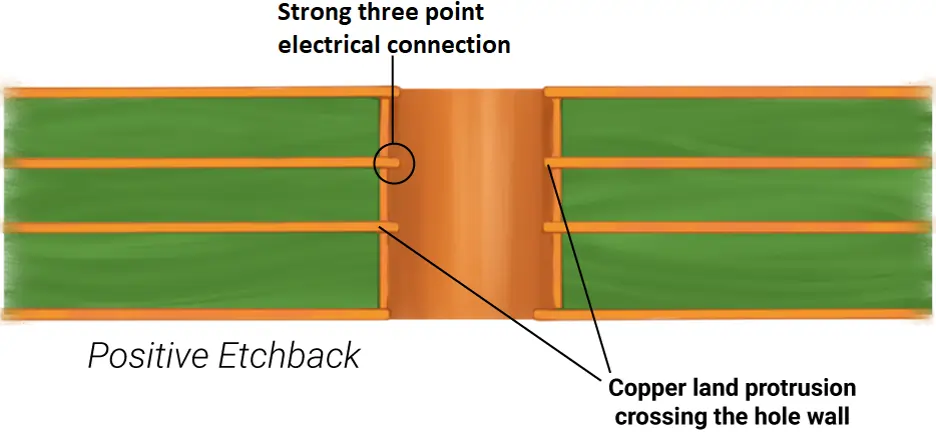
🎯 How to Solve Impedance Issues in HDI PCBs Without Redesigning the Whole Board?
This is a question we get a lot. The answer? Think ahead—before you even route a trace.
-
Use controlled impedance tools to define trace width and dielectric constants.
-
Follow a PCB stackup strategy that supports high-speed signals. We recommend placing ground planes adjacent to signal layers.
-
Avoid discontinuities—like sharp corners or sudden width changes.
-
Partner with a manufacturer who understands signal integrity in HDI PCB production.
📏 What Are the Critical HDI PCB Via Design Rules for Multilayer Boards?
In multilayer HDI boards, via design is everything. Here’s what matters:
-
Microvias should follow a 1:1 aspect ratio for reliability.
-
Use blind vias to connect surface to inner layers, and buried vias for internal routing.
-
If you stack vias, ensure each layer is properly laser drilled and filled.
-
Stick to IPC 2226 standards—they’re not optional. When designing microvia structures, we strictly adhere to IPC-2226 guidelines, which define design standards for HDI interconnections, via reliability, and stackup configurations.
💡 Pro tip: Avoid stacking more than 2 microvias deep without copper filling or support.
🧠 How to Plan HDI Stackup Design for High-Speed Applications?
Your stackup is your foundation.
-
Alternate power and ground planes to reduce EMI.
-
Use low-loss dielectric materials to maintain signal speed and reduce crosstalk.
-
Place sensitive signals in the inner layers for protection.
-
Consider HDI PCB layout tools that simulate performance before fabrication.
📊 Chart 2: Good vs. Bad Stackup Example
| Feature | Good Stackup | Poor Stackup |
|---|---|---|
| Signal Layer Shielding | Ground/power shielding | Unshielded |
| Dielectric | Low-loss, balanced | High-loss, inconsistent |
| Via Planning | Blind, buried, staggered | Random full drills |
| Impedance Control | Simulated & measured | Assumed or ignored |
🔧 What Are the Top Challenges in HDI PCB Manufacturing—and How Do We Fix Them?
We hear this a lot: “My last HDI board failed post-reflow.”
Here’s where things go wrong in HDI PCB manufacturing:
1. Microvia Cracking
A common failure due to thermal cycling. We use sequential lamination and reliable copper fill to reinforce weak vias.
2. Delamination Issues
Too much heat during lamination ruins the stack. We strictly control lamination profiles and material prep.
3. Registration Misalignment
With so many layers, one misaligned drill can trash the whole board. We use automated optical alignment systems.
So yes, HDI PCB challenges are real—but they’re not unbeatable.
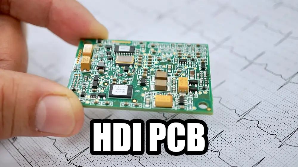
🚀 How Turnkey HDI PCB Assembly Solves Time and Quality Problems for Prototyping
Outsourcing isn’t just about saving money—it’s about saving time, rework, and frustration.
We offer fast HDI PCB prototyping services with:
-
Same-day quoting
-
In-house DFM checks
-
100% functional testing
-
HDI PCB low-volume manufacturing in China with local engineering teams
📊 Chart 3: DIY vs. Turnkey HDI PCB Prototyping
| Metric | DIY | Turnkey (Our Service) |
|---|---|---|
| Time to Quote | 2–3 days | <12 hours |
| Error Rate | Higher | Lower (DFM Verified) |
| Cost Per Unit (Low Volume) | High | Optimized |
| Engineering Support | None | Included |
The result? Your boards work the first time—and get to market faster.
Our turnkey HDI PCB prototyping service isn’t just about speed—it’s also about cost control and first-pass success. If you’re not using a unified service yet, here’s why turnkey PCB assembly services can revolutionize your business.
🛠️ Industry Pain Points We Hear Every Day (And How Our Services Solve Them)
“My last PCB partner ghosted me.”
“Can’t get low-volume quotes that make sense.”
“Why does my board pass simulation but fail in real life?”
Sound familiar?
We’ve built our turnkey HDI PCB assembly in China to address these exact pain points:
-
Fast quoting—even for small runs
-
Transparent engineering feedback
-
Clear stackup and via rules before fab
-
Dedicated account manager to walk you through each build
You don’t need to be an expert—we’ll handle the heavy lifting. If you’re exploring HDI PCB low-volume manufacturing in China, choosing the right partner is critical. Here’s what you must know when selecting a reliable HDI PCB manufacturer in China—from MOQ policies to communication, quality, and delivery consistency.
FAQs
1. What is HDI in PCB design, and why is it used?
HDI (High-Density Interconnect) in PCB design refers to circuit boards with higher wiring density achieved through technologies like microvias, blind/buried vias, and fine traces. It’s used in high-speed and compact applications—think smartphones, wearables, and aerospace—where space-saving, signal integrity, and performance are critical. HDI PCB layout ensures better routing density and controlled impedance for high-speed designs.
2. What are the main problems in HDI PCB design, and how do you fix them?
Common HDI PCB design problems include microvia reliability, impedance mismatches, signal loss, and crosstalk. Solutions involve proper HDI stackup design for high-speed applications, precise HDI PCB via design rules for multilayer boards, and simulation-driven impedance control. Partnering with a manufacturer that supports IPC-2226 and laser drilling ensures better performance and yield.
3. How do you reduce crosstalk and parasitic effects in HDI PCBs?
To reduce crosstalk in HDI PCBs, follow the 3W rule: keep spacing between signal traces at least three times their width. Use ground planes to isolate high-speed signals and avoid parallel routing on adjacent layers. Also, minimize parasitic capacitance by limiting overlapping copper areas and avoiding unnecessary via stubs.
4. What’s the difference between HDI and standard PCB materials and structure?
HDI PCBs use advanced materials like polyimide or high-Tg FR4 to support fine pitch components and thermal stress. Unlike standard PCBs with through-hole vias, HDI boards rely on microvia vs through-hole strategies to achieve multilayer interconnects in tight spaces. This leads to lighter, thinner, and more robust performance—ideal for modern electronics.
Have Specific Requirements?
Looking for high-precision PCB assembly for your products? Our team specializes in delivering top-tier assembly services, ensuring your devices perform flawlessly in any environment. Contact us today for a free consultation on how we can enhance your product’s reliability.
🧾 Summary
HDI PCB design is complicated—but it doesn’t have to be painful. We’ve solved these issues for companies across industries. If any of the above challenges sound familiar, reach out and let’s build smarter together.
Save on your next PCB project?
Claim $100 OFF your order today.
✅ high-quality PCB assembly with strict quality control ✅ ISO-certified & 8+ years of experience. ✅ Low MOQ, fast turnaround, and 100% E-tested PCBs.
Additional Resources:
- How to Repair Circuit Boards: A Step-by-Step Beginner’s Guide
- Capacitor on Circuit Board: A Comprehensive Guide
- What Are PCB Conformal Coatings? Types, Benefits, and Applications Explained
- SMD Size Codes Explained: A Complete Guide to Understanding Surface-Mount Component Dimensions
- AC vs DC: Key Differences, Applications, and Advantages in Modern Electronics
Request for Quote
RECENT POSTS
IC Boards Explained: Applications, Layout Tips, and Assembly Services
Discover what IC boards are, how they’re used in modern electronics, and how to design
HDI PCB vs Multilayer PCB: How to Choose the Right One for Cost, Signal Integrity & Manufacturing
HDI PCB vs multilayer PCB explained from a manufacturing and assembly perspective. Learn how cost,
RELATED POSTS
Leading PCBA Manufacturer
✅ Assemble 20 PCBAS for $0 ✅ Get $100 OFF – Risk-Free Trial!
✅ 100+ Satisfied Customers
✅ Ensured Quality & On-Time Delivery
✅ Free Trial, No Commitments!
