Quick Leads-PCBA
High-density interconnect PCBs are the heart of today’s compact, high-performance devices—yet sourcing them can feel like pulling teeth. Between high minimum order quantities, slow lead times, and complicated communication loops, many engineers and procurement managers are stuck waiting or overpaying. If that’s familiar, let me walk you through why partnering with an HDI PCB manufacturer in China might be the game-changer you’ve been looking for.
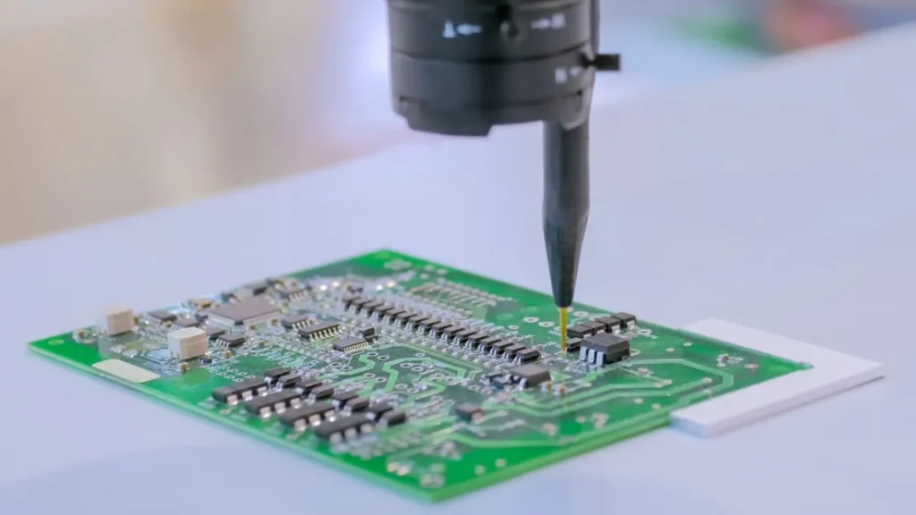
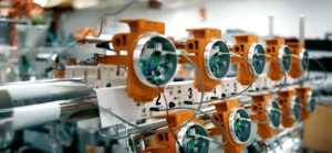
Chinese HDI PCB manufacturers offer low or no minimum order quantities, fast-turn fabrication, and complete turnkey assembly—ideal for prototyping and low-volume production. With advanced microvia, blind/buried via, and controlled impedance technologies, they deliver high-layer count, compact PCBs quickly and cost-effectively. These solutions are crucial for industries like medical, telecom, and IoT.
Let’s explore the core pain points in sourcing HDI PCBs—and how China’s ecosystem is not only solving them but pushing boundaries.
What Are the Pain Points in HDI PCB Sourcing Today?
For many professionals I talk to—whether you’re in R&D, supply chain, or project management—the struggle is real. Here are the three biggest headaches that come up over and over again:
1. High Minimum Order Quantities (MOQ)
It’s frustrating when you just want to prototype or run a small batch but suppliers won’t budge below 1,000 units. The risk? You’re stuck with inventory you might never use.
2. Lead Times That Don’t Work for Development Cycles
Fast-moving projects don’t have the luxury of waiting 4–6 weeks for board fabrication. Quick-turn HDI PCB fabrication in China? That can mean as fast as 5 working days.
3. Lack of Transparency or Technical Support
With some offshore suppliers, it feels like you’re playing a game of broken telephone. You send in a Gerber file and get boards back, but no clarity on DFM issues or suggestions for optimization.
Why Choose an HDI PCB Manufacturer in China?
Let me break this down visually. Here’s how Chinese HDI PCB suppliers compare with typical Western counterparts:
| Feature | Western Manufacturers | HDI PCB Manufacturer China |
|---|---|---|
| MOQ Requirements | 500–1000 units | 0–10 units |
| Lead Time | 15–30 business days | 5–10 business days |
| Turnkey Assembly | Sometimes available | Often integrated |
| Cost per Unit (Low Volume) | $$$ | $$ |
| Support for Prototyping | Limited | Strong, fast quoting systems |
These aren’t just numbers—they reflect a manufacturing ecosystem built for flexibility, which is exactly what fast-paced industries need.
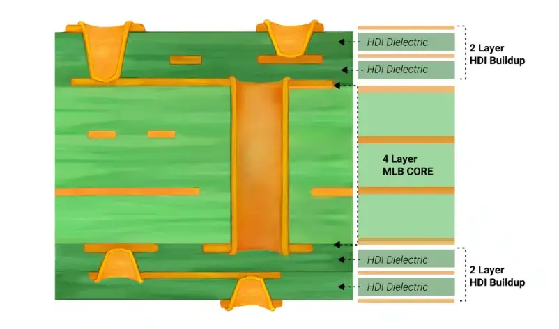
What Is HDI PCB and Why Is It So Important?
If you’re reading this, you’re likely already familiar with the basics, but let’s quickly recap for context.
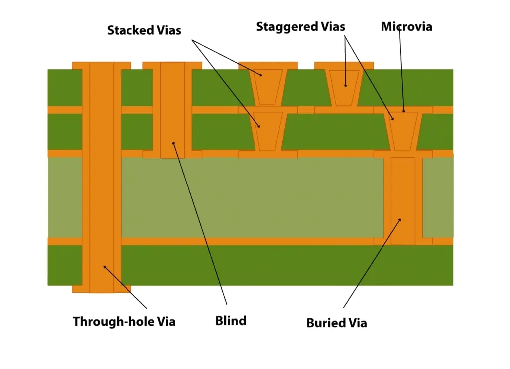
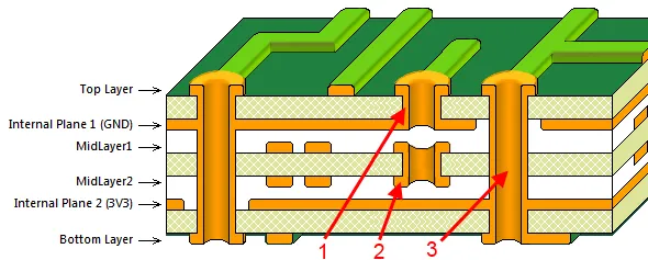
HDI (High Density Interconnect) PCBs use:
Microvias for increased routing density
Blind and buried vias to reduce board size
Via-in-pad PCB design to accommodate fine-pitch components
Advanced layer stack-up designs for multi-layer boards
These techniques enable designers to pack more functionality into smaller spaces without compromising on signal integrity.
📌 HDI technology is essential in sectors like medical electronics, automotive, aerospace, wearables, and smartphones.
When you’re working with compact form factors or high-speed signals, standard PCBs just won’t cut it. You need fine-line PCB manufacturing and precise impedance control. According to IPC-2226A, HDI PCBs follow specific microvia and lamination design standards that ensure high-density interconnect performance and reliability.
How Does Quick-Turn HDI PCB Fabrication Work in China?
This is one of the biggest reasons engineers prefer Chinese partners for time-sensitive projects.
Here’s a typical quick-turn flow:
| Process Step | Turnaround Time |
|---|---|
| Quote & DFM Feedback | 0.5–1 day |
| CAM & Tooling | 1 day |
| Lamination & Drilling (Microvia, Blind/Buried) | 2 days |
| Plating & Imaging | 1 day |
| Surface Finishing | 1 day |
| QA + Shipping | 1–2 days |
That’s under 7 working days if you’re dealing with a responsive HDI PCB manufacturer for prototyping in China.
Unit Circuits: Leading PCBA Manufacturer
 ISO-certified & 8+ years of PCBA Low MOQ & Fast Turnaround Prototype & Mass production
Limited Time Offer:
Get $100 off your order TODAY!
What Technical Capabilities Should You Look For?
Let’s go a bit deeper technically because the devil is in the details when you’re building controlled impedance HDI PCBs. Reliable manufacturers adhere to industry standards like IPC Board Design Guidelines to ensure trace width control, impedance accuracy, and overall HDI reliability.
Look for these specs:
Microvia Diameter: Down to 0.1mm
Trace Width/Spacing: As low as 3/3 mil
Layer Count: 4 to 20+ layers
Stack-Up: 1+N+1, 2+N+2, even 4+N+4
Impedance Tolerance: ±10% typical
Solder Mask Registration: ±3 mil
Surface Finishes: ENIG, ENEPIG, OSP, etc.
If you’re sourcing for PCB for compact electronic devices, this level of precision is non-negotiable.
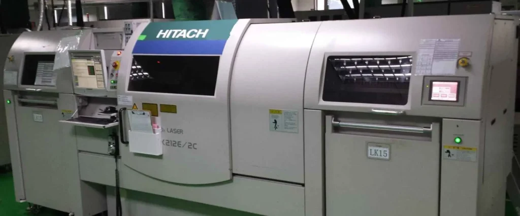
🧠 Tip: Ask if they support laser drilling for stacked microvias and automated optical inspection (AOI) for each layer.
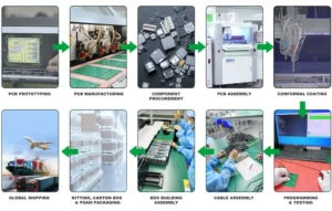
Can You Really Get Turnkey HDI PCB Assembly in China?
Short answer? Yes.
Long answer? It depends on the supplier. But more and more HDI PCB manufacturers in China now offer one-stop services:
Component sourcing (including hard-to-find ICs)
SMT line compatibility with fine-pitch BGAs
Functional testing & in-circuit testing
Conformal coating and enclosure assembly
When you opt for HDI PCB with turnkey assembly in China, you remove an entire layer of coordination. That’s especially valuable when working with low-volume PCB production for startups or specialized applications.
Many Chinese factories now provide end-to-end service—from stack-up design to functional testing. If you’re still managing fabrication and assembly separately, check out this overview on why turnkey PCB assembly can transform your workflow.
No MOQ: Is It Real? What’s the Catch?
It’s not a scam, I promise.
HDI PCB no minimum order offers are real—but you’ll need to understand what comes with it:
| Pros | Trade-Offs |
|---|---|
| Ideal for prototyping | Slightly higher cost per unit |
| Zero inventory risk | May limit customization options |
| Super fast quote-to-order | Fewer payment term negotiations |
This is where Chinese suppliers shine, especially for fine-line or high-layer count PCB builds.
How Are Chinese Manufacturers Supporting Medical, Automotive & IoT?
It’s not just about volume. Chinese manufacturers are delivering certified, traceable, and audit-friendly production—especially for regulated markets.
Use cases:
Medical Electronics: HDI PCBs with biocompatible coatings and tight signal tolerance
Automotive: Rigid-flex HDI boards in sensor modules and ADAS units
IoT Devices: Ultra-compact designs with via-in-pad layouts and low-loss materials
Many of these projects require close collaboration—so having in-house DFM and FAE support makes a big difference.
Prototyping HDI Boards? Here’s What to Know
If you’re looking for an HDI PCB manufacturer for prototyping, your focus is on speed, flexibility, and iteration. Chinese suppliers now offer:
Online quoting tools with instant stack-up previews
24–48 hour build options for basic HDI layouts
Integrated DRC/DFM analysis included in the cost
BOM kitting + passive sourcing on request
This agility is unmatched—and it can reduce your total product cycle by 30% or more. For time-sensitive R&D or IoT pilots, speed matters. Want a head start on who’s leading the pack? Check out this curated list of top quick-turn PCB assembly companies in 2025.
How to Evaluate a Reliable HDI PCB Partner in China
Don’t just look at price. Here’s a checklist we use internally when sourcing:
✅ ISO 9001, ISO 13485, IATF 16949 certifications
✅ In-house microvia and blind/buried via capabilities
✅ Stack-up engineering support
✅ Clear lead time breakdowns
✅ Fluent communication with CAM/DFM teams
✅ Transparent quoting (no hidden tooling fees)
✅ Experience with signal integrity in HDI builds
If they pass all of the above, they’re worth a pilot run. Choosing the right partner requires more than price comparisons. Look for experience with impedance control, certifications, and customer support. Here’s a full guide on how to choose a reliable PCB supplier in China for long-term success.
FAQs
1. Who is the best HDI PCB manufacturer in China for fast, low-volume orders?
If you're seeking an HDI PCB manufacturer in China with no MOQ, quick-turn fabrication, and turnkey assembly, look for those offering in-house microvia drilling, stack-up design, and component sourcing. Chinese suppliers like PCBWay, Hemeixin, and smaller agile factories excel in HDI PCB with component sourcing—ideal for prototyping and R&D runs.
2. What is the difference between standard PCB and HDI PCB?
Standard PCBs use traditional vias and spacing, while HDI PCBs incorporate blind and buried vias, microvias, and fine-line PCB manufacturing to support compact, multi-layer designs. This enables better signal integrity in HDI and allows for higher interconnect density—critical in wearables, IoT, and medical devices.
3. Why are HDI PCBs more expensive—and are they worth it?
HDI PCB fabrication in China may cost more than standard PCBs due to laser drilling, tighter tolerances, and controlled impedance requirements. However, for high-performance or space-constrained applications, they're worth every penny—delivering compact size, faster signals, and fewer layers overall. That translates to smarter, lighter products.
4. What are the advantages of using HDI PCBs for medical or telecom applications?
HDI PCBs offer superior electrical performance, space efficiency, and reliability—making them ideal for medical electronics and telecom gear. Technologies like via-in-pad, layer stack-up HDI, and low-loss materials allow precise routing in small spaces, which improves signal clarity and reduces failure risk in mission-critical devices.
Have Specific Requirements?
Looking for high-precision PCB assembly for your products? Our team specializes in delivering top-tier assembly services, ensuring your devices perform flawlessly in any environment. Contact us today for a free consultation on how we can enhance your product’s reliability.
Final Thoughts
China’s HDI PCB manufacturers are uniquely positioned to meet the technical and business demands of today’s fast-paced electronics world. Whether you need low-volume prototyping or full-scale production, they offer fast, flexible, and turnkey services with no compromise on quality.
If you’re tired of delays, MOQs, and unclear quotes, it’s time to explore a smarter path forward.
Save on your next PCB project?
Claim $100 OFF your order today.
✅ high-quality PCB assembly with strict quality control ✅ ISO-certified & 8+ years of experience. ✅ Low MOQ, fast turnaround, and 100% E-tested PCBs.
Additional Resources:
- How to Repair Circuit Boards: A Step-by-Step Beginner’s Guide
- Capacitor on Circuit Board: A Comprehensive Guide
- What Are PCB Conformal Coatings? Types, Benefits, and Applications Explained
- SMD Size Codes Explained: A Complete Guide to Understanding Surface-Mount Component Dimensions
- AC vs DC: Key Differences, Applications, and Advantages in Modern Electronics
Request for Quote
RECENT POSTS
IC Boards Explained: Applications, Layout Tips, and Assembly Services
Discover what IC boards are, how they’re used in modern electronics, and how to design
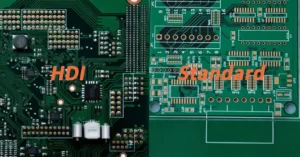
HDI PCB vs Multilayer PCB: How to Choose the Right One for Cost, Signal Integrity & Manufacturing
HDI PCB vs multilayer PCB explained from a manufacturing and assembly perspective. Learn how cost,
RELATED POSTS
Leading PCBA Manufacturer
✅ Assemble 20 PCBAS for $0 ✅ Get $100 OFF – Risk-Free Trial!
✅ 100+ Satisfied Customers
✅ Ensured Quality & On-Time Delivery
✅ Free Trial, No Commitments!