Quick Leads-PCBA
The Real Story Behind Fast, No-MOQ HDI PCB Services
HDI PCBs are the invisible engine behind today’s compact, high-performance electronics—but making them right isn’t easy. As an engineer or sourcing manager, you’re probably juggling design complexities, lead time pressure, and reliability demands. I’ve been there. So let me show you the real, full-scope OEM process—and where you can skip the pain.
What Is HDI PCB Manufacturing?
HDI PCB manufacturing involves high-density interconnect techniques using blind and buried vias, microvias, and fine-pitch routing. The OEM process includes schematic design, multilayer stack-up, laser drilling, copper plating, SMT assembly, and quality testing such as AOI and X-ray inspection. No MOQ services offer flexibility, while turnkey manufacturing ensures faster time-to-market.
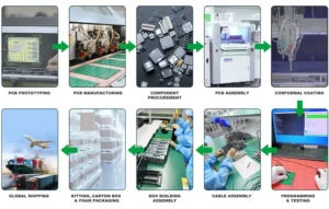
From Schematic to Shipment: How to Manufacture HDI PCB Step by Step
Let’s break down the full OEM process behind HDI PCB fabrication. These aren’t generic steps—they’re what we run every day for clients like you.
-
Schematic Design & DFM Review
You send us your design files (Gerber, BOM, pick-and-place), and we conduct Design for Manufacturability (DFM) checks to prevent issues later. -
Multilayer Stack-Up Planning
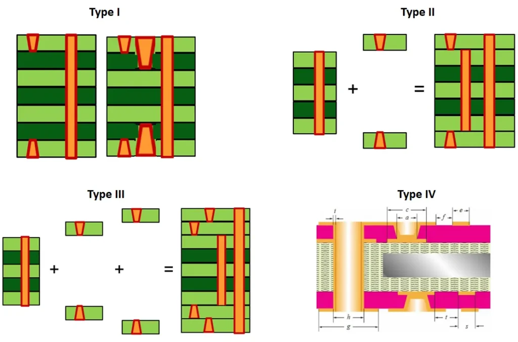
For HDI PCBs, layer stack-up is everything. We use high-Tg FR4, polyimide, or hybrid materials depending on thermal and impedance needs. Expect between 6–12 layers for most OEMs. We align all design parameters with IPC-2226A, the industry standard for HDI layouts and stack-up rules view standard. -
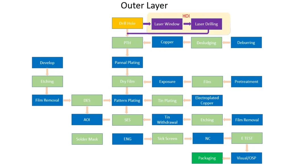
Laser Drilling & Microvias
Blind and buried vias are drilled using lasers with micron-level precision. This minimizes layer misalignment and improves electrical performance. -
Copper Plating & Via Filling
Next, we plate the copper and fill microvias (often with conductive or non-conductive resin). This supports fine-pitch components and high signal integrity. -
Pattern Imaging & Etching
After lamination, copper traces are imaged and etched—controlled impedance routing is key here, especially for RF and high-speed apps. -
Solder Mask, Silkscreen & Surface Finish
ENIG, OSP, or Immersion Silver—your board gets the finish it needs depending on shelf life and assembly requirements. -
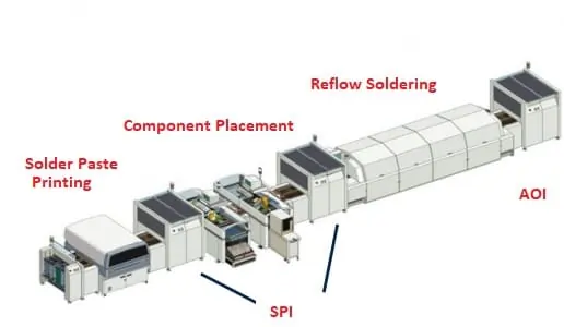
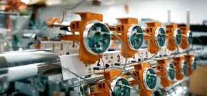
SMT Assembly (Turnkey)
We source components (or you can supply them), then run full SMT on our high-speed lines. We also support BGA, PoP, and 01005 placement. -
Testing & QC
AOI, flying probe, electrical testing, and even X-ray for BGA packages. We don’t let a board ship unless it passes everything.
Why HDI PCBs Are the Backbone of OEM Electronics Production
When we talk about HDI PCB for OEM products, it’s not just marketing. These boards are designed for:
-
Wearables & IoT (small size, high speed)
-
Industrial automation (high EMI tolerance)
-
Medical devices (IPC Class 3 reliability)
-
Aerospace & automotive (complex multilayer reliability)
Problem: Traditional PCBs just can’t handle the density and miniaturization.
Our Advantage: We specialize in turnkey PCB manufacturing that supports everything from RF shielding to controlled impedance routing.
📊 Traditional PCB vs HDI PCB
| Feature | Traditional PCB | HDI PCB |
|---|---|---|
| Layer Count | 2–6 | 6–16+ |
| Vias | Through-hole | Blind, buried, microvias |
| Density | Moderate | High |
| Impedance Control | Limited | Advanced (±10%) |
| Minimum Trace Width | ≥ 6mil | ≥ 3mil |
| Application Suitability | Consumer electronics | Industrial, Aerospace, Medical |
Unit Circuits: Leading PCBA Manufacturer
 ISO-certified & 8+ years of PCBA Low MOQ & Fast Turnaround Prototype & Mass production
Limited Time Offer:
Get $100 off your order TODAY!
OEM PCB vs EMS: What’s the Difference?
You may have heard both terms thrown around—but here’s how I explain it to clients:
-
OEM PCB: You (the OEM) design the board, and we build it.
-
EMS (Electronics Manufacturing Services): We handle the whole process—design tweaks, component sourcing, SMT, testing.
We offer both. If you’ve got a completed design and just want no MOQ PCB assembly, we’ve got your back. If you’re starting from a rough idea, we can walk it into production together.
What Are the Pain Points in HDI PCB Production Today?
Even veteran engineers run into these:
-
Layer Misregistration: Leads to signal loss or total failure.
-
Stack-up Delamination: Caused by poor lamination pressure or mismatched materials.
-
Component Sourcing Delays: Global shortages affect timeline & cost.
-
Assembly Errors (BGA): You can’t inspect what you can’t see—unless you have X-ray.
We solve these by:
-
Using automated AOI + X-ray on all complex builds
-
Having onshore and offshore sourcing teams in Shenzhen for real-time part availability
-
Running daily calibration on lamination and drill equipment
From Prototype to Production: Fast, Low-Volume PCB Manufacturing in China
There’s a myth that fast = sloppy. Here’s how we do fast PCB prototyping service without cutting corners:
-
DFM review within 24 hours
-
Component sourcing in parallel with production
-
Next-day SMT lines for confirmed files
-
99.5% yield rate, even in quick-turn batches
📊 Quick-Turn HDI PCB Providers in China
| Provider | MOQ | Turnaround | X-ray Inspection | Cost ($ for 4-layer, 50 pcs) |
|---|---|---|---|---|
| Us | None | 2–5 working days | Yes | $320–$350 |
| PCBWay | 5 pcs | 5–7 days | Optional | $400+ |
| JLCPCB | 5 pcs | 6–8 days | No | $360+ |
| Rayming | 10 pcs | 7–9 days | Yes | $420+ |
| Hilelectronic | 20 pcs | 7–10 days | No | $450+ |
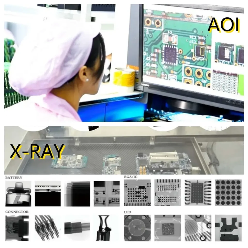
HDI PCB Testing: What’s Actually Included?
A lot of shops skip this—or charge extra. We don’t.
-
AOI (Automated Optical Inspection) – for every panel
-
Flying Probe Electrical Testing – checks open/short circuits
-
X-ray Inspection – standard for all BGA packages
-
IPC Class 2/3 Compliance – available on request
These ensure your board doesn’t just look good—it works reliably, especially in industrial or medical environments.
How Fast is “Fast” Turnaround?
Turnaround depends on board complexity and size. Here’s a rough guide:
-
< 50 pcs, ≤ 1m²: 24–48 hrs
-
1–5m²: 3–4 days
-
5–10m²: 5–6 days
-
10m²+: 7+ days
We keep priority lanes open for quick-turn HDI PCB assembly service clients. Just flag it in the quote.
PCBA vs PCB: Which One Do You Actually Need?
-
PCB: Just the bare board
-
PCBA: PCB + components + full assembly
If you’re doing OEM electronics production, you almost always need PCBA unless you have in-house lines. We do both—and help with sourcing components from China too.
JLCPCB, PCBWay, Rayming: How We Compare
We respect the big players. But our edge lies in personal service, no hidden fees, and true “no MOQ” support.
Want the best EMS company in China for HDI PCB? Choose a team that offers:
-
Dedicated engineer feedback
-
Built-in testing
-
Transparent quotes
-
Real human support
FAQs
1. What is PCB functional testing and why does it matter in HDI PCB assembly?
PCB functional testing simulates real-world operating conditions to ensure the assembled board performs as intended. For HDI PCB assembly, this test verifies complex routing, high-frequency signals, and power delivery. It’s especially critical in OEM electronics production, where performance failures can lead to costly recalls. Our turnkey PCB manufacturing process includes functional testing by default.
2. How do you test for polychlorinated biphenyls (PCBs) in materials?
While unrelated to printed circuit boards, polychlorinated biphenyls (PCBs) are toxic industrial chemicals often found in outdated equipment. They're tested using analytical methods for PCBs, like gas chromatography and mass spectrometry. If you're importing materials from older suppliers in China, it's wise to request certification. Our components meet RoHS and REACH safety compliance.
3. What are the four types of system-level tests for electronics?
System-level testing goes beyond PCB testing. It includes:
Functional tests to simulate operation,
Stress tests for thermal and electrical loads,
Integration tests for multi-board systems, and
End-of-line (EOL) testing before packaging.
These help ensure your low volume PCB manufacturing project doesn’t fail once integrated into your final OEM product.
4. How does HDI PCB design impact signal integrity and trace width rules?
HDI PCB designs improve signal integrity by reducing parasitic capacitance and inductance—thanks to controlled impedance routing and shorter trace lengths via microvias. But these benefits come with tight constraints: trace width and spacing rules must follow IPC standards, especially in high-speed or RF applications. We assist clients in balancing performance and manufacturability.
Have Specific Requirements?
Looking for high-precision PCB assembly for your products? Our team specializes in delivering top-tier assembly services, ensuring your devices perform flawlessly in any environment. Contact us today for a free consultation on how we can enhance your product’s reliability.
Final Thoughts: Build Something Better
HDI PCB manufacturing isn’t just about fitting more in less space. It’s about doing it right—reliably, efficiently, and with a team that knows what matters to OEMs.
If you’re sourcing, scaling, or just prototyping something new, let’s talk. We’ll show you what fast, flexible, and fail-proof really looks like.
Choosing the right HDI PCB manufacturer in China—especially one offering no MOQ and full turnkey PCB assembly—can dramatically speed up your time-to-market. Here’s a guide on how to pick wisely: read more.
Save on your next PCB project?
Claim $100 OFF your order today.
✅ high-quality PCB assembly with strict quality control ✅ ISO-certified & 8+ years of experience. ✅ Low MOQ, fast turnaround, and 100% E-tested PCBs.
Additional Resources:
- How to Repair Circuit Boards: A Step-by-Step Beginner’s Guide
- Capacitor on Circuit Board: A Comprehensive Guide
- What Are PCB Conformal Coatings? Types, Benefits, and Applications Explained
- SMD Size Codes Explained: A Complete Guide to Understanding Surface-Mount Component Dimensions
- AC vs DC: Key Differences, Applications, and Advantages in Modern Electronics
Request for Quote
RECENT POSTS
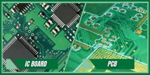
IC Boards Explained: Applications, Layout Tips, and Assembly Services
Discover what IC boards are, how they’re used in modern electronics, and how to design
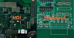
HDI PCB vs Multilayer PCB: How to Choose the Right One for Cost, Signal Integrity & Manufacturing
HDI PCB vs multilayer PCB explained from a manufacturing and assembly perspective. Learn how cost,
RELATED POSTS
Leading PCBA Manufacturer
✅ Assemble 20 PCBAS for $0 ✅ Get $100 OFF – Risk-Free Trial!
✅ 100+ Satisfied Customers
✅ Ensured Quality & On-Time Delivery
✅ Free Trial, No Commitments!