Quick Leads-PCBA
 Looking for full-service PCB Assembly?
Turnkey solutions from PCB manufacturing to testing.
sales@unitcircuits.com
Modern electronics design no longer fails at the schematic level—it fails at the manufacturing and assembly interface. I’ve seen many projects stall, not because engineers chose the “wrong” chipset, but because they underestimated how the choice between HDI PCB vs multilayer PCB would ripple through SMT placement, soldering yield, testing strategy, and long-term reliability. If you’re sourcing PCB assembly services, this decision affects far more than routing density or board size.
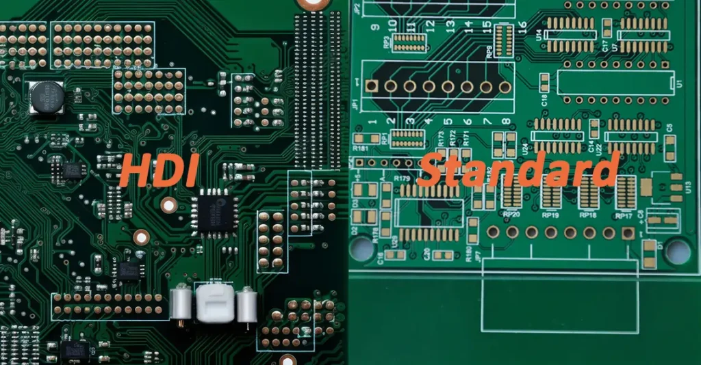
HDI PCBs offer higher wiring density, microvia-based interconnections, and shorter signal paths that benefit high-speed and miniaturized designs, while standard multilayer PCBs remain more cost-effective and easier to assemble for many applications. The correct choice depends not on PCB type alone, but on total manufacturing cost, assembly yield, and long-term reliability requirements.
Choosing the right board structure isn’t about following trends. It’s about understanding where HDI adds real value—and where it quietly creates manufacturing risk. Let’s walk through this decision the way an experienced EMS partner would, starting from today’s real industry pain points.
The Design–Manufacturing Disconnect Is the Root Cause of Most PCBA Failures
One of the most persistent issues in electronics manufacturing is the design–manufacturing gap. Designs pass ERC, DRC, and signal simulations, yet problems surface the moment the board enters SMT.
The reason is simple: design rules are not manufacturing rules.
HDI designs amplify this gap. Microvia stacks, via-in-pad structures, and ultra-fine pitch components may be electrically sound, but they place extreme demands on solder paste printing, placement accuracy, and thermal profiling. Without early DFM analysis, yield losses become inevitable.
Experienced HDI manufacturers consistently emphasize that ultra-dense designs require fabrication and assembly constraints to be addressed early, a point echoed by Sierra Circuits in their discussion of ultra-HDI PCB design and fabrication challenges.
From a PCB assembly perspective, the biggest risks include:
-
Insufficient solder mask dam width around fine-pitch pads
-
Poor via filling quality leading to solder voiding
-
Pad cratering during rework
-
Limited inspection access, forcing heavy reliance on X-ray
A multilayer PCB with controlled impedance often tolerates far more variation during assembly. This is why experienced OEM electronics manufacturing teams always evaluate assembly feasibility before committing to HDI.
Many HDI issues don’t come from schematic mistakes, but from how dense layouts interact with real manufacturing tolerances. In practice, problems such as stacked microvia reliability, solder voiding, and rework limitations are far more common than most designers expect, especially without early assembly-driven design review. Some of the most frequent HDI design pitfalls—and how engineers mitigate them in production—are outlined in this practical breakdown of real HDI PCB design problems.
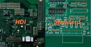
Difference Between HDI and Multilayer PCB — Beyond the Marketing Definitions
Most articles stop at definitions. That’s not helpful when you’re making a sourcing decision.
The real difference between HDI and multilayer PCB becomes obvious only after the board hits the production line.
Structural Differences That Directly Affect Assembly Yield
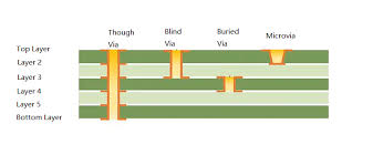
HDI PCBs rely on:
-
Microvia technology (blind, buried, stacked, or staggered)
-
Sequential lamination cycles
-
Thinner dielectrics and tighter registration tolerances
These features allow impressive routing density, but they also:
-
Reduce mechanical robustness
-
Increase sensitivity to thermal stress
-
Limit rework options
By contrast, a standard multilayer PCB uses through-hole vias and larger capture pads. From an SMT and DIP assembly standpoint, this means:
-
More stable solder joints
-
Easier AOI coverage
-
Lower scrap risk during rework
Why HDI PCB vs Standard Multilayer PCB Is Really an Assembly Question
Electrically, HDI often wins. Manufacturing-wise, it’s conditional.
High-density layouts increase placement accuracy requirements, reduce stencil design margin, and make solder joint inspection more complex. If your EMS partner is not equipped for consistent microvia-based assembly, HDI can quietly destroy yield.
Unit Circuits: Leading PCBA Manufacturer
 ISO-certified & 8+ years of PCBA Low MOQ & Fast Turnaround Prototype & Mass production
Limited Time Offer:
Get $100 off your order TODAY!
sales@unitcircuits.com
Rising Signal Integrity Requirements — But HDI Is Not Required for Every Design
There’s a dangerous assumption in today’s market: high-speed equals HDI. That’s not always true.
For many designs, especially below certain data-rate thresholds, a properly designed impedance controlled PCB using traditional multilayer stackups delivers excellent signal integrity without the complexity of HDI.
Leading EDA providers also note that increased routing density does not automatically mandate HDI, especially when signal integrity targets can be met through stackup and impedance control strategies, as discussed in Cadence’s analysis of high-density PCB design.
HDI becomes justified when:
-
Escape routing for dense BGAs is impossible otherwise
-
Trace length reduction materially improves eye diagrams
-
EMI cannot be controlled with layer stack optimization alone
However, I’ve reviewed many designs where HDI was selected prematurely, driving up cost and assembly risk without measurable signal improvement.
This is where experienced PCBA partners push back—not to reduce performance, but to avoid over-engineering that hurts manufacturability.
HDI PCB Cost vs Multilayer PCB Cost — Why Unit Price Is the Wrong Metric
Comparing HDI PCB cost vs multilayer PCB cost based on fabrication quotes alone is one of the most common sourcing mistakes.
The real cost difference emerges during assembly and testing.Many sourcing teams compare HDI PCB cost vs multilayer PCB cost purely on fabrication quotes, only to discover later that assembly yield, rework, and delivery delays drive total cost far higher than expected. In real production environments, the cheapest PCBA option frequently introduces hidden risks that outweigh any initial savings—a pattern that becomes especially visible when examining the true cost of low-price PCB assembly decisions.
A lower-cost PCB can quickly become expensive due to:
-
SMT yield loss from fine-pitch defects
-
Increased rework labor
-
Higher scrap rates
-
Extended lead times from repeated process tuning
From a total manufacturing cost (TCO) perspective, the cheapest PCB often produces the most expensive PCBA.
This is also where low-cost, platform-driven procurement models fail. They optimize for unit price, not production stability—a mismatch for companies building real products at scale.
HDI PCB Manufacturing Process — Where Complexity Begins
Understanding the HDI PCB manufacturing process explains why assembly risk rises.
Each sequential lamination step introduces:
-
Registration drift
-
Cumulative thermal stress
-
Increased warpage risk
Laser-drilled microvias must be perfectly filled and plated. Any inconsistency affects:
-
Pad flatness
-
Solder paste volume
-
Joint reliability
These manufacturing realities directly impact downstream SMT processes. Without coordination between PCB fabrication and assembly teams, HDI designs become fragile.
This is why serious buyers look for HDI PCB manufacturing and assembly under one coordinated quality system—not fragmented sourcing.

Increasing Assembly Density — When PCBA Yield Becomes the Bottleneck
As component density increases, PCBA yield—not PCB design—becomes the limiting factor.
High-density layouts challenge:
-
Stencil thickness optimization
-
Solder paste release consistency
-
Pick-and-place accuracy at scale
In multilayer PCB SMT and DIP assembly, engineers have room to adjust. In HDI PCB assembly, margins shrink dramatically.
Yield losses typically appear as:
-
Bridging on fine-pitch components
-
Head-in-pillow defects on BGAs
-
Latent failures after thermal cycling
These are not beginner issues—they are systemic challenges that only surface in volume production.
HDI PCB Assembly Considerations Most Designers Learn Too Late
Effective HDI PCB assembly considerations must start early.
Critical checkpoints include:
-
Via-in-pad filling and planarization quality
-
Solder mask registration capability
-
Component sourcing tolerances
-
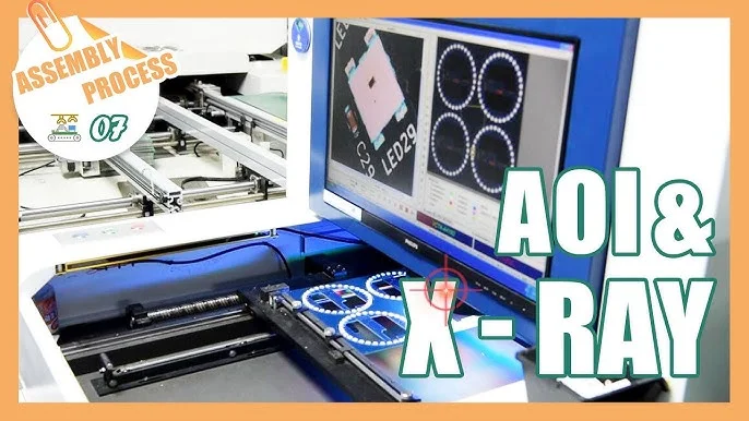
AOI and X-ray inspection strategy
Skipping these discussions often leads to expensive redesigns. This is why professional HDI PCB assembly services emphasize pre-production reviews rather than post-failure fixes.
From “Can It Be Built?” to “Can It Be Built Reliably Over the Long Term?”
Short-term assembly success does not equal long-term reliability.
HDI structures are more susceptible to:
-
Microvia fatigue
-
Thermal expansion mismatch
-
Solder joint stress concentration
For products expected to operate for years, functional testing and reliability validation are not optional. A robust PCBA process includes:
-
Electrical testing
-
Functional testing
-
Stress screening where appropriate
This is where HDI PCB with testing services separates professional manufacturing from transactional assembly.
Choosing Between HDI PCB Assembly Services and Multilayer PCB Assembly Services
So how do you choose?
HDI PCB assembly services make sense when:
-
Miniaturization is mandatory
-
Signal integrity requirements are proven
-
Volumes justify process optimization
Multilayer PCB assembly services are often better when:
-
Cost stability matters
-
Reliability margins are critical
-
Designs allow routing flexibility
For many OEMs, turnkey HDI PCB assembly reduces risk by consolidating responsibility—but only when the provider understands both fabrication and assembly deeply.
When You Should NOT Choose HDI — A Reality Check for Cost-Driven Projects
HDI is not a universal upgrade.
If your project is:
-
Extremely price-sensitive
-
Low to mid complexity
-
Tolerant of larger board size
Then HDI likely introduces more problems than it solves. This isn’t a limitation of HDI—it’s a reminder that engineering decisions must match business reality.
Teams that habitually chase the lowest PCBA price often discover too late that manufacturing shortcuts create hidden costs. Serious production requires serious process control.
FAQs
1. How do I know if my project truly needs HDI PCB instead of a standard multilayer PCB?
Many projects are pushed toward HDI prematurely. If your design meets signal integrity targets using controlled impedance multilayer routing, HDI may not be necessary. HDI PCB vs multilayer PCB decisions should be based on routing feasibility, component density, and assembly yield—not trends. A quick DFM and assembly review often reveals whether HDI adds real value or only increases HDI PCB cost and manufacturing risk.
2. What assembly risks are most common when switching from multilayer PCB to HDI PCB?
The most frequent issues include solder bridging on fine-pitch components, insufficient via-in-pad filling, and inspection limitations requiring X-ray. HDI PCB assembly considerations differ significantly from multilayer PCB SMT and DIP assembly. Without process tuning and testing strategy alignment, yield loss—not PCB fabrication—becomes the main bottleneck in HDI PCB manufacturing and assembly.
3. Why do some HDI PCB assembly services reject “PCB-only” designs from low-cost platforms?
Low-cost PCB sources often optimize fabrication price, not assembly compatibility. In HDI PCB assembly services, microvia quality, solder mask accuracy, and flatness directly affect yield. Designs optimized only for PCB cost frequently cause rework, delays, or failures during SMT. Professional multilayer PCB assembly services and turnkey HDI PCB assembly providers prioritize total manufacturing stability, not unit PCB pricing.
4. Should testing requirements influence the choice between HDI PCB and multilayer PCB?
Yes. Testing strategy is often overlooked during board selection. HDI PCB with testing services typically requires greater reliance on X-ray, boundary scan, or functional testing due to limited probe access. Multilayer PCBs usually allow simpler electrical test coverage. When reliability and lifecycle cost matter, testing complexity should be evaluated alongside signal integrity and PCB structure.
Have Specific Requirements?
Looking for high-precision PCB assembly for your products? Our team specializes in delivering top-tier assembly services, ensuring your devices perform flawlessly in any environment. Contact us today for a free consultation on how we can enhance your product’s reliability.
Summary
Choosing between HDI and multilayer PCB is not about technology preference—it’s about manufacturing outcomes. When cost, yield, signal integrity, and long-term reliability are evaluated together, the right answer becomes clear. The best results come from aligning design intent with proven PCB assembly and soldering expertise from the very beginning.
Save on your next PCB project?
Claim $100 OFF your order today.
sales@unitcircuits.com
✅ high-quality PCB assembly with strict quality control ✅ ISO-certified & 8+ years of experience. ✅ Low MOQ, fast turnaround, and 100% E-tested PCBs.
Additional Resources:
- How to Repair Circuit Boards: A Step-by-Step Beginner’s Guide
- Capacitor on Circuit Board: A Comprehensive Guide
- What Are PCB Conformal Coatings? Types, Benefits, and Applications Explained
- SMD Size Codes Explained: A Complete Guide to Understanding Surface-Mount Component Dimensions
- AC vs DC: Key Differences, Applications, and Advantages in Modern Electronics
Request for Quote
sales@unitcircuits.com
RECENT POSTS
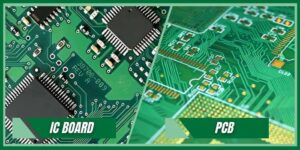
IC Boards Explained: Applications, Layout Tips, and Assembly Services
Discover what IC boards are, how they’re used in modern electronics, and how to design
HDI PCB vs Multilayer PCB: How to Choose the Right One for Cost, Signal Integrity & Manufacturing
HDI PCB vs multilayer PCB explained from a manufacturing and assembly perspective. Learn how cost,
RELATED POSTS
Leading PCBA Manufacturer
✅ Assemble 20 PCBAS for $0 ✅ Get $100 OFF – Risk-Free Trial!
sales@unitcircuits.com
✅ 100+ Satisfied Customers
✅ Ensured Quality & On-Time Delivery
✅ Free Trial, No Commitments!