Quick Leads-PCBA
🔹 Introduction: The Cost of Getting It Wrong
Lead-free PCB assembly isn’t just about checking a RoHS compliance box. It’s a delicate balance of chemistry, heat, timing, and layout — and thermal management sits at the heart of it all.
As someone who’s spent years working with engineers sourcing RoHS-compliant PCB assemblies, I’ve seen firsthand how poor thermal profiling leads to cold joints, lifted pads, and even full board failures. It’s not just frustrating — it’s expensive.
Let’s break down why PCB thermal management matters more than ever in the lead-free era, and how to get it right from the start.
✅ What is thermal profiling in PCB assembly?
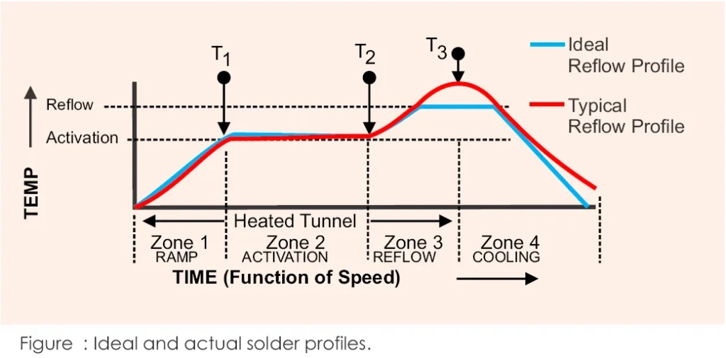
At its core, thermal profiling is the process of measuring and controlling how heat is applied to a PCB during soldering — especially reflow soldering.
In lead-free assembly, where solder paste (typically SAC305) melts at higher temperatures than traditional tin-lead, this becomes crucial. We’re talking peak reflow temperatures around 245–250°C. Push too hot, and you risk delamination or component warping. Go too cold, and hello, cold joints.
Think of thermal profiling as creating a heat “storyline” — from preheat to soak to reflow and cool-down. Every component and every solder pad has to hit the right temperature at the right moment.
🔧 Thermal Profiling Tools:
Thermocouples (attached directly to solder joints)
Profiling software (to map out ramp rates and peak windows)
Convection reflow ovens with zoned control
According to a detailed study by IEEE on thermal behavior in lead-free solder joints, maintaining optimal heating and cooling rates significantly improves long-term solder joint reliability.
✅ Why is thermal management important in PCB design?
Here’s the hard truth: PCB design that ignores heat is just waiting to fail.
High component density, power-hungry ICs, and multi-layer boards can trap heat like a sauna. If you don’t plan for heat dissipation, the result isn’t pretty — cracked vias, degraded components, or intermittent BGA failures that are brutal to diagnose.
⚠️ Industry Pain Points:
| Challenge | Consequence |
|---|---|
| Tight component spacing | Heat hotspots |
| No thermal relief in vias | Difficult reflow |
| Poor heat-sink layout | Shorter component life |
| Inconsistent pad sizes | Uneven heating during soldering |
💡 What works:
Use thermal relief vias for power planes
Account for component heat tolerance during layout
Model thermal stress in PCB simulations early
“We use pre-assembly DFM checks and simulation tools to flag potential hotspots before production even starts. It saves a lot of rework down the line.”
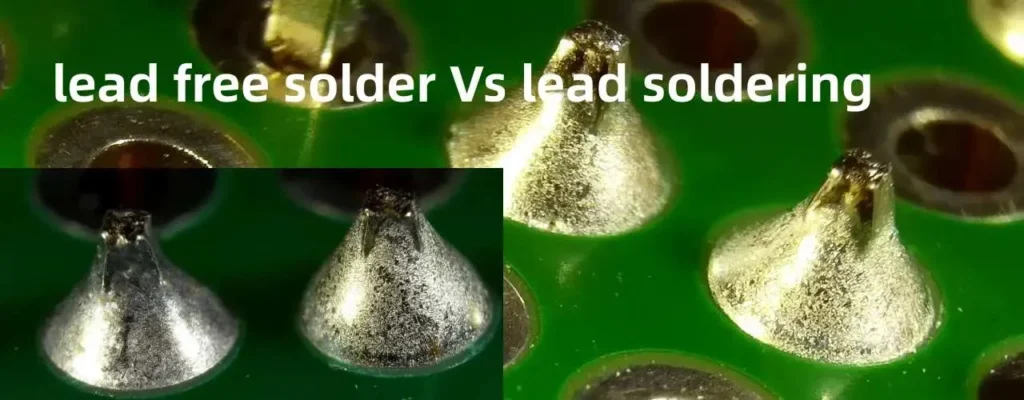
✅ How does lead-free soldering impact PCB assembly?
Lead-free soldering brings a few more challenges than traditional tin-lead. For starters, it needs higher temperatures. But that’s only the beginning.
As highlighted in a PCD&F article on lead-free assembly, transitioning from tin-lead to SAC-based solder significantly impacts reflow profile and defect rates.
| Parameter | Leaded | Lead-Free (SAC305) |
|---|---|---|
| Melting Point | ~183°C | ~217°C |
| Peak Reflow Temp | ~210°C | 245–250°C |
| Oxidation Risk | Low | Higher |
| Defect Sensitivity | Lower | Higher |
That extra heat puts stress on both components and the board itself — especially when you’re working with fine-pitch BGA, ceramic capacitors, or temperature-sensitive connectors.
RoHS-compliant PCB designs also need to be checked for component ratings, as not all parts can handle those reflow conditions.
The shift from leaded to lead-free soldering isn’t just about regulation — it fundamentally changes how heat interacts with your assembly. This comparison between lead and lead-free solder breaks down thermal, reliability, and material implications clearly.
✅ What are common thermal issues in PCBs?
Here’s what I’ve seen in poorly managed lead-free processes:
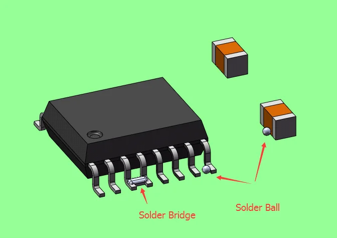
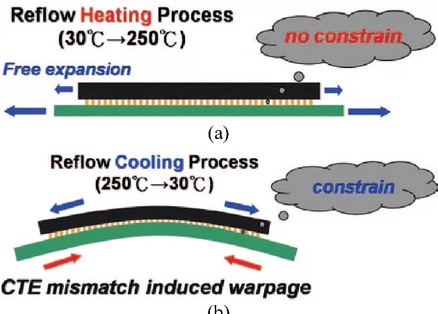
Warped PCBs: Caused by uneven heating or thin board materials
Solder voids: Often from trapped moisture or wrong soak time
Cold joints: Ramp-up too slow or peak temp too low
Tombstoning: Uneven pad sizes or asymmetrical heating
Common Defects vs. Root Causes
| Defect | Cause | Fix |
|---|---|---|
| Cold joints | Inadequate peak temp | Adjust reflow profile |
| Solder voids | Moisture or flux outgassing | Bake boards, improve soak |
| BGA head-in-pillow | Poor wetting, oxidized balls | Optimize soak zone |
| PCB warpage | Thin layers, fast temp change | Use thicker boards, gradual heating |
Unit Circuits: Leading PCBA Manufacturer
 ISO-certified & 8+ years of PCBA Low MOQ & Fast Turnaround Prototype & Mass production
Limited Time Offer:
Get $100 off your order TODAY!
✅ Why thermal profiling is important in lead-free PCB assembly
This is where many engineers go wrong. They apply a standard leaded solder reflow profile to a lead-free assembly and hope it works. It doesn’t.
Lead-free profiles have stricter thermal requirements, especially during:
Preheat zone (to reduce thermal shock)
Soak zone (for flux activation and even heating)
Reflow peak (where actual soldering happens)
Cool-down (to avoid brittle joints)
🧠 Tip: Document the thermal profile used and validate it with thermocouple measurements. This isn’t just good practice — it’s a requirement for surface mount reliability.
✅ Best temperature profile for lead-free soldering
Every assembly is different, but for SAC305, here’s a common reference:
| Zone | Temperature Range | Duration |
|---|---|---|
| Preheat | 150–180°C | 60–120 sec |
| Soak | 180–200°C | 60–120 sec |
| Reflow | 240–250°C (peak) | 30–60 sec |
| Cooling | Down to ~100°C | Gradual |
✅ Keep ramp-up rate under 3°C/sec
✅ Soak evenly to prevent tombstoning
✅ Use thermal cycling testing post-assembly for reliability assurance
Getting the reflow profile right isn’t just about peak temperature — it’s about the entire thermal curve. From ramp-up to cool-down, every second counts. If you’re working with SAC305 solder, these SMT reflow soldering tips will help you avoid tombstoning, cold joints, and board stress.
✅ How to avoid cold joints in RoHS soldering
Cold joints are sneaky. They might pass inspection but fail in the field. They’re typically caused by:
Low peak temperatures
Inadequate flux activation
Fast cooling
To avoid them:
Use a well-profiled convection oven
Choose the right preheat and soak zones
Monitor with real-time profiling tools
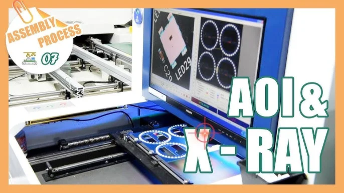
We run X-ray inspection and AOI on every critical solder joint — especially BGA — and match it to thermal data. That’s how we keep yields high.
✅ Lead-free soldering defects and solutions
Let’s list out the usual suspects:
| Defect | Fix |
|---|---|
| Solder Balling | Reduce flux or adjust ramp-up |
| Voids | Improve paste storage, use vacuum reflow |
| Head-in-Pillow | Use correct reflow time & ball alloy |
| Bridging | Check stencil design, paste volume |
| Delamination | Lower peak or reduce ramp rate |
📍 Key takeaway: lead-free assembly is less forgiving — precision matters.
✅ Choosing a China PCB assembly RoHS lead-free supplier
Not all suppliers are created equal.
Here’s what to ask before placing an order:
Do they offer thermal profiling documentation?
What inspection systems are used (AOI, X-ray, ICT)?
Can they meet your chosen reflow profile?
Do they conduct thermal cycling or stress testing?
Working with a custom lead-free PCB manufacturer with thermal testing means you’re not flying blind — you’re backed by data.
✅ Low MOQ PCB assembly with lead-free process
We often get startups or R&D clients asking for low-MOQ PCB assembly — and yes, you can get RoHS lead-free builds even for 5–10 pieces.
But here’s the key:
Make sure your supplier offers the same thermal profiling and testing rigor for low-volume as they do for mass production.
Otherwise, that prototype may not scale well later.
FAQs
1. What are the basics of thermal management in PCB design?
Thermal management in PCB design involves strategies to control heat buildup from components during operation. It includes proper copper thickness, thermal vias, and optimized layout. In lead-free PCB assembly, managing heat becomes even more critical due to higher reflow temperatures. Without effective thermal control, issues like PCB warpage, cold joints, or reduced surface mount reliability can occur — affecting long-term performance.
2.What causes increased heat in lead-free PCB assembly?
Higher peak reflow temperatures required for SAC305 lead-free solder naturally generate more thermal stress. Add to that dense layouts, poor airflow, and inefficient copper balancing — and you’ve got a recipe for overheating. Components with low heat tolerance are at risk, especially in designs lacking preheat and soak zone tuning or proper thermal profiling.
3. What are common PCB assembly defects and how can they be prevented?
In lead-free soldering, typical defects include solder voids, cold joints, and head-in-pillow BGA issues. These often stem from poorly managed thermal profiles. To avoid them, use precision SMT reflow profiles, choose quality solder paste, and ensure consistent thermal cycling testing. Partnering with a custom lead-free PCB manufacturer with thermal testing reduces these risks dramatically.
4. How is thermal management handled during PCB prototyping with low MOQ?
Even in low MOQ PCB assembly, skipping thermal validation is a mistake. Reliable China PCB assembly RoHS suppliers provide the same thermal profiling tools — including reflow ovens with zone control and real-time monitoring — used in full production. This ensures small-batch RoHS-compliant PCB builds are just as robust, helping you avoid redesigns later.
Have Specific Requirements?
Looking for high-precision PCB assembly for your products? Our team specializes in delivering top-tier assembly services, ensuring your devices perform flawlessly in any environment. Contact us today for a free consultation on how we can enhance your product’s reliability.
✅ Why work with a custom lead-free PCB manufacturer with thermal testing?
Because thermal failures aren’t always immediate.
A supplier who runs in-house profiling, logs real-time oven data, and offers thermal cycling testing is giving you way more than just a PCB. They’re giving you confidence.
We’ve helped clients eliminate cold joints, reduce field failures, and speed up time to market — all through smarter thermal strategies.
🔹 Conclusion: Get Heat Right, Get Results
Thermal profiling isn’t optional — it’s your invisible quality inspector.
From preheat zones to component heat tolerance, every temperature step counts. Whether you’re prototyping or scaling to production, success in lead-free PCB assembly begins with heat done right.
If you’re looking for a China-based RoHS-compliant PCB assembly supplier that doesn’t cut corners on thermal management, we’re ready to help.
Need help with your next lead-free build?
Get in touch — we’ll share a sample thermal profile or walk you through our process.
Save on your next PCB project?
Claim $100 OFF your order today.
✅ high-quality PCB assembly with strict quality control ✅ ISO-certified & 8+ years of experience. ✅ Low MOQ, fast turnaround, and 100% E-tested PCBs.
Additional Resources:
- How to Repair Circuit Boards: A Step-by-Step Beginner’s Guide
- Capacitor on Circuit Board: A Comprehensive Guide
- What Are PCB Conformal Coatings? Types, Benefits, and Applications Explained
- SMD Size Codes Explained: A Complete Guide to Understanding Surface-Mount Component Dimensions
- AC vs DC: Key Differences, Applications, and Advantages in Modern Electronics
Request for Quote
RECENT POSTS
IC Boards Explained: Applications, Layout Tips, and Assembly Services
Discover what IC boards are, how they’re used in modern electronics, and how to design
HDI PCB vs Multilayer PCB: How to Choose the Right One for Cost, Signal Integrity & Manufacturing
HDI PCB vs multilayer PCB explained from a manufacturing and assembly perspective. Learn how cost,
RELATED POSTS
Leading PCBA Manufacturer
✅ Assemble 20 PCBAS for $0 ✅ Get $100 OFF – Risk-Free Trial!
✅ 100+ Satisfied Customers
✅ Ensured Quality & On-Time Delivery
✅ Free Trial, No Commitments!