Quick Leads-PCBA
 Looking for full-service PCB Assembly?
Turnkey solutions from PCB manufacturing to testing.
sales@unitcircuits.com
High-speed multilayer PCBs are the backbone of modern electronics—but signal distortion, EMI, and assembly mismatches can quietly destroy performance. Many buyers still rely on low-cost, DFM-ignorant suppliers, worsening the issue. This guide reveals expert design rules and real solutions to help you ensure noise-free, production-ready multilayer PCB performance.
To achieve noise-free performance in multilayer PCBs, engineers must apply expert signal integrity design rules: optimized layer stackup, controlled impedance routing, differential pair planning, and EMI-conscious layout. Turnkey PCB assembly services that include DFM reviews and pre-simulation can catch potential issues early—ensuring consistent signal quality from design through production.
Let’s dive deeper into the technical design rules, industry pain points, and practical solutions that ensure every high-speed multilayer PCB you source delivers reliable, noise-free performance.
🔧 How do you ensure signal integrity in a PCB?
Signal integrity in a high-speed multilayer PCB depends on disciplined planning. Controlled impedance routing ensures traces don’t reflect signals. Return path optimization, matched differential pairs, and precise trace length tuning help maintain waveform integrity across the board.
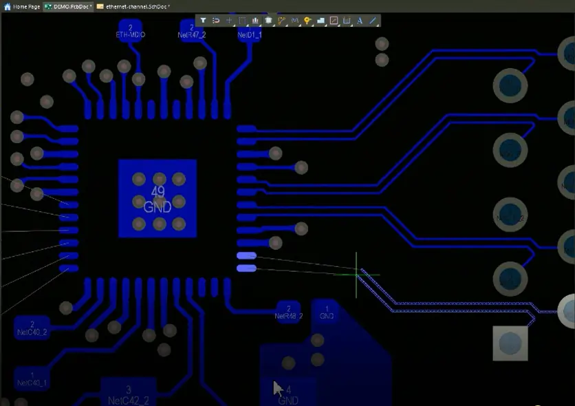
We typically use differential pair design rules, via stub elimination, and crosstalk prevention in PCB layout. Impedance calculators are applied during layout to set trace width and spacing in coordination with the dielectric material.
Engineers use techniques like controlled impedance routing, minimizing signal reflection, and proper stack-up to ensure signal quality as outlined by Altium.
📌 Tip: Use signal integrity analysis tools like HyperLynx or Altium SI to simulate transmission line behavior before layout is finalized.
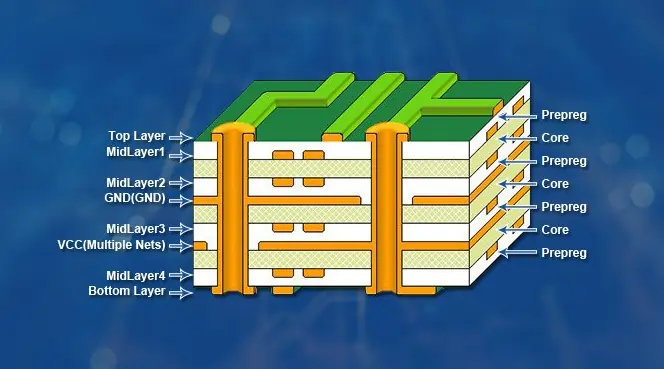
📐 What is the recommended PCB stackup for signal integrity?
A good multilayer PCB stackup design for signal quality features alternating signal and ground layers. For high-speed applications, 6 to 12-layer designs are common. Here’s a simplified example:
-
Top Layer: Signal
-
Layer 2: Ground Plane
-
Layer 3: Signal
-
Layer 4: Power Plane
-
Layer 5: Ground Plane
-
Bottom Layer: Signal
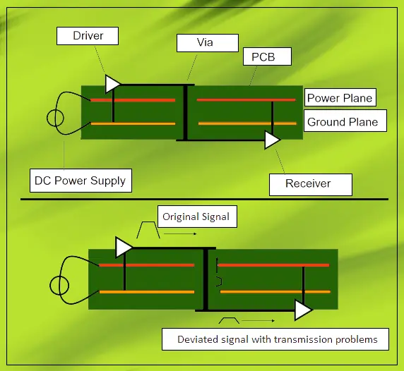
This layout shortens return paths and shields signals from EMI, contributing to higher signal integrity.
Avoid split ground planes—they introduce impedance discontinuities. Always consider stackup simulation to validate assumptions before manufacturing.
🔊 How does multilayer PCB reduce noise?
Multilayer PCBs excel in EMI suppression by enabling compact, low-inductance signal paths. Ground planes act as EMI shields, and adjacent signal layers minimize loop areas.
Our low noise multilayer PCB design service involves early-stage simulation, layout rules based on the target bandwidth, and thermal analysis. These steps are critical for reducing long-term board failure due to high-frequency ringing or interference.
Boards designed with noise immunity in mind experience up to 30% fewer failures during EMC testing, according to our internal DFM case studies.
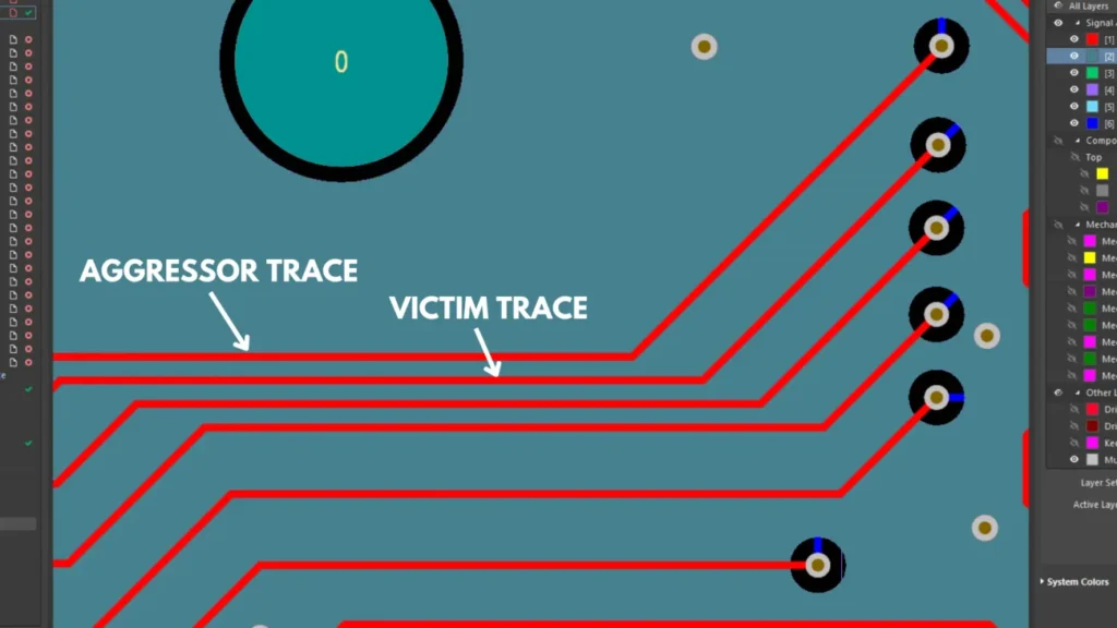
⚠️ What causes signal integrity issues in high-speed PCB design?
Signal integrity issues arise when electrical and physical design elements are misaligned:
-
Poor layer stackup without defined return paths
-
Uncontrolled impedance variation due to inconsistent trace widths
-
Lack of differential pair symmetry
-
Via stubs causing signal reflection
-
Excessively long or unshielded traces
Many of these issues are seen in projects that prioritize low cost over performance. A 2025 IEEE study showed a 40% increase in EMI susceptibility in boards with unbalanced stackups.
Many signal issues stem from avoidable layout and assembly flaws—like those listed in the top 8 common PCB assembly problems, from poor soldering to misaligned pads.
Unit Circuits: Leading PCBA Manufacturer
 ISO-certified & 8+ years of PCBA Low MOQ & Fast Turnaround Prototype & Mass production
Limited Time Offer:
Get $100 off your order TODAY!
sales@unitcircuits.com
🛠️ Multilayer PCB EMC Design Considerations
Designing for EMC is not optional—it’s essential. At the board level, use:
-
Continuous ground planes under all signal traces
-
Via stitching around sensitive nets
-
Decoupling capacitors placed close to power pins
-
Split planes carefully managed for analog-digital isolation
We also include return path optimization, especially for clock and differential pairs. Controlled impedance routing directly contributes to better EMC performance.
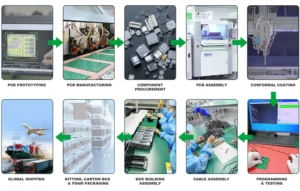
🔄 Turnkey SMT and Thru-Hole Assembly in China: What to Look For?
True turnkey PCB assembly with signal integrity support means much more than just soldering. Look for providers who offer:
-
DFM review of Gerbers and BOM
-
Stackup consultation with impedance targets
-
In-house signal testing before and after SMT
-
Experience with mixed assembly: SMT + thru-hole
Choosing a turnkey SMT and thru-hole assembly in China with technical depth ensures that high-speed design requirements are not lost during production.
At UnitCircuits, we bridge design and manufacturing by keeping everything under one review process.
A turnkey PCB assembly service simplifies stackup validation, DFM reviews, and testing under one roof—minimizing errors and speeding time-to-market.
🧠 Simulation Before Fabrication: How Important Is It?
Pre-fab simulation has become non-negotiable in the age of USB 3.0, CAN FD, and HDMI interfaces. You can avoid late-stage surprises by validating:
-
Trace impedance using tools like a PCB trace impedance calculator
-
EMI hotspots with 2D/3D field solvers
-
Differential pair skew and return path discontinuities
Most of our custom multilayer PCB with assembly projects begin with a simulation file, not a layout file. Studies like this IEEE analysis show how pre-fabrication signal integrity simulation can reduce EMI and timing errors by addressing via stub resonance and impedance mismatch early in the process.
🚫 Why Low-Cost PCBA Suppliers Often Fail Signal Integrity Tests
Some PCBA providers emphasize volume and pricing over technical quality. Here’s what we’ve observed from customer feedback:
-
Stackups are rarely simulated
-
No impedance verification post-assembly
-
Uncoordinated design + assembly, leading to solder defects
-
Generic material use, not optimized for signal speed
To be clear, we do not support sourcing habits focused on low-cost prototyping platforms with no quality control for high-speed needs.
Instead, we recommend working with a china PCB assembly manufacturer for high-speed boards who validates stackup, routing, and soldering at every step.
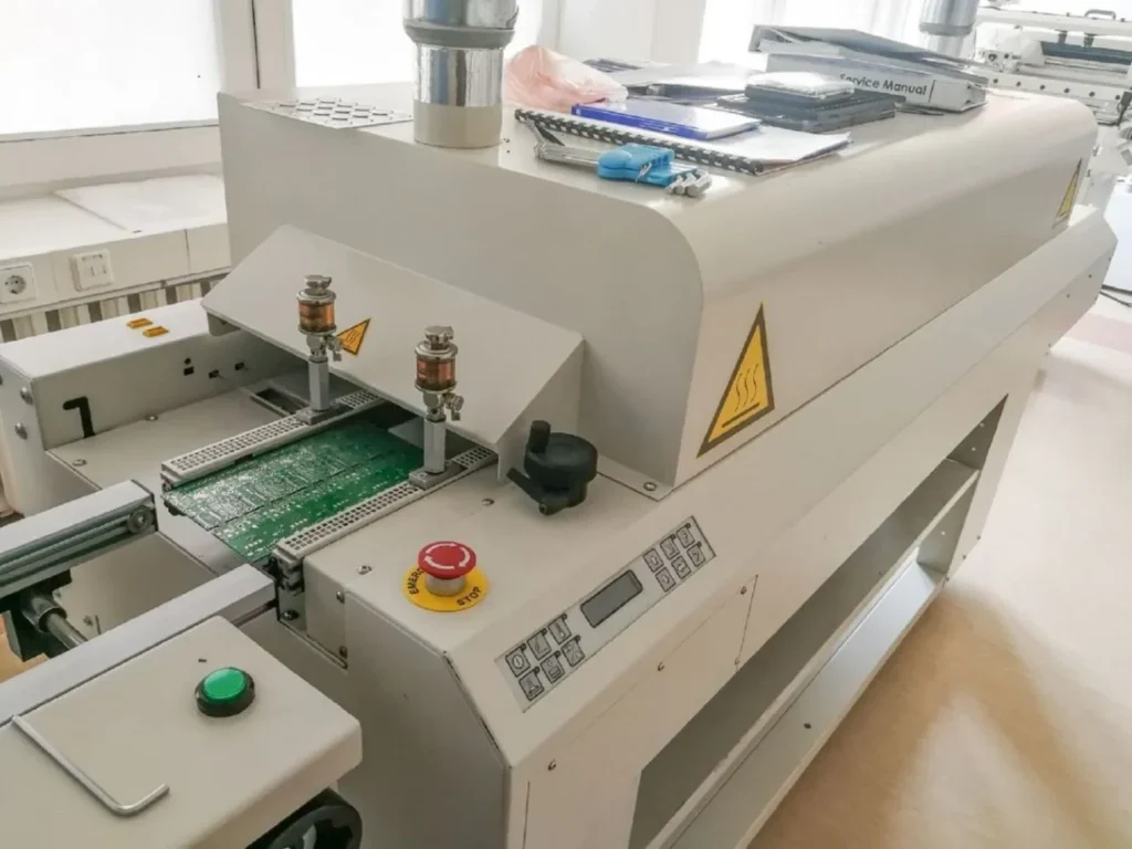
⚙️ Solving SMT & Soldering Challenges in High-Speed Boards
High-frequency boards are more vulnerable to SMT defects caused by minor layout inconsistencies:
-
Solder bridging due to fine pitch parts
-
BGA voiding because of insufficient paste
-
Misalignment in wave soldering PCB service stages
We use X-ray inspection and thermal profiling to solve these. For industrial control PCB assembly services, we also run pre-functional testing.
From stencil design to reflow profile matching, every step must be optimized for impedance integrity and solder joint reliability.
📈 How One-Stop Services Reduce Rework and Speed Time-to-Market
Split vendors = miscommunication. Delays. Surprises.
One-stop partners offering PCB design and assembly one stop service eliminate these problems by aligning stackup recommendations, solder paste specs, and testing methods.
We support no MOQ PCB assembly with testing, which allows rapid prototyping without risking quality—especially helpful for high-reliability sectors like telecom and industrial controls.
FAQs
1. What should I check before sending my multilayer PCB for assembly?
Before assembly, verify the stackup meets your signal integrity requirements, and confirm your Gerber files align with DFM standards. Pay attention to trace impedance, component placement, and via structures. A custom multilayer PCB with assembly service can help review these in advance—reducing rework risk and saving time.
2. Can turnkey PCB services handle both SMT and wave soldering in one order?
Yes, a qualified turnkey SMT and wave soldering PCB service can manage mixed-technology boards. This is essential for designs requiring both SMD and through-hole components. With the right partner, you’ll streamline production and improve board-level reliability—especially valuable in industrial or automotive applications.
3. How does impedance control affect PCB performance during testing?
Impedance mismatches lead to signal reflection, EMI issues, and test failures. Using pcb impedance control for signal integrity ensures each trace meets strict tolerances, reducing debugging time. Look for vendors offering impedance-controlled fabrication and in-circuit testing to catch issues before final delivery.
4. Is no-MOQ PCB assembly reliable for high-speed board development?
Absolutely—reputable services offering no MOQ PCB assembly with testing often specialize in prototyping and small-batch runs for high-speed multilayer boards. They provide full process control, stackup consultation, and post-assembly validation to ensure quality—ideal for startups and R&D teams aiming for fast market entry.
Have Specific Requirements?
Looking for high-precision PCB assembly for your products? Our team specializes in delivering top-tier assembly services, ensuring your devices perform flawlessly in any environment. Contact us today for a free consultation on how we can enhance your product’s reliability.
✅ Summary
Want noise-free performance and lower project risk? Choose a high-speed PCB assembly partner who understands signal integrity from the inside out. Let’s help you go from prototype to production—faster, with fewer design revisions, and zero surprises.
📎 Contact us today for custom stackup simulation, turnkey SMT solutions, and high-speed multilayer PCB fabrication trusted by engineers worldwide.
Save on your next PCB project?
Claim $100 OFF your order today.
sales@unitcircuits.com
✅ high-quality PCB assembly with strict quality control ✅ ISO-certified & 8+ years of experience. ✅ Low MOQ, fast turnaround, and 100% E-tested PCBs.
Additional Resources:
- How to Repair Circuit Boards: A Step-by-Step Beginner’s Guide
- Capacitor on Circuit Board: A Comprehensive Guide
- What Are PCB Conformal Coatings? Types, Benefits, and Applications Explained
- SMD Size Codes Explained: A Complete Guide to Understanding Surface-Mount Component Dimensions
- AC vs DC: Key Differences, Applications, and Advantages in Modern Electronics
Request for Quote
sales@unitcircuits.com
RECENT POSTS
IC Boards Explained: Applications, Layout Tips, and Assembly Services
Discover what IC boards are, how they’re used in modern electronics, and how to design
HDI PCB vs Multilayer PCB: How to Choose the Right One for Cost, Signal Integrity & Manufacturing
HDI PCB vs multilayer PCB explained from a manufacturing and assembly perspective. Learn how cost,
RELATED POSTS

Leading PCBA Manufacturer
✅ Assemble 20 PCBAS for $0 ✅ Get $100 OFF – Risk-Free Trial!
sales@unitcircuits.com
✅ 100+ Satisfied Customers
✅ Ensured Quality & On-Time Delivery
✅ Free Trial, No Commitments!