Quick Leads-PCBA
💡 Looking for full-service PCB Assembly?
We offer turnkey solutions from PCB manufacturing to testing.
Many electronics teams struggle with delays, waste, and misalignment during SMT and THT assembly. These issues often trace back to poor PCB layout and handling. Fortunately, panelization solves this by optimizing the entire process—from component placement to soldering and testing—making it faster, cheaper, and more scalable.
PCB panelization is the process of grouping multiple boards into a single panel for streamlined assembly. It enhances throughput, reduces handling errors, and simplifies machine setup—particularly during SMT and THT stages. By optimizing layout for pick-and-place, reflow, and wave soldering, panelization minimizes waste and speeds up production, ultimately lowering total manufacturing costs.
Let’s explore the pain points in modern PCB assembly and how smart panelization strategies—and turnkey services—are solving them across industries.
What is PCB Panelization and Why is It Important?
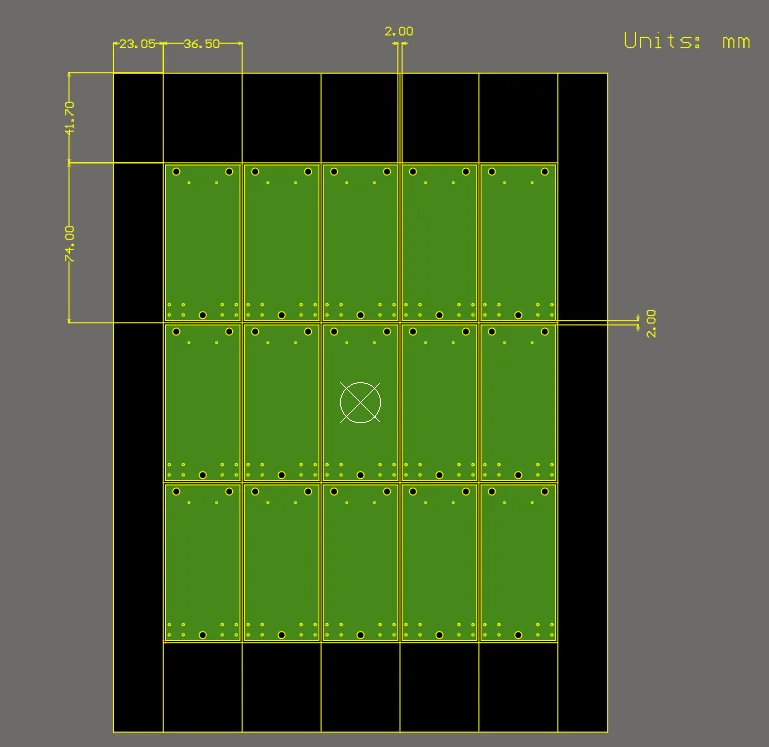
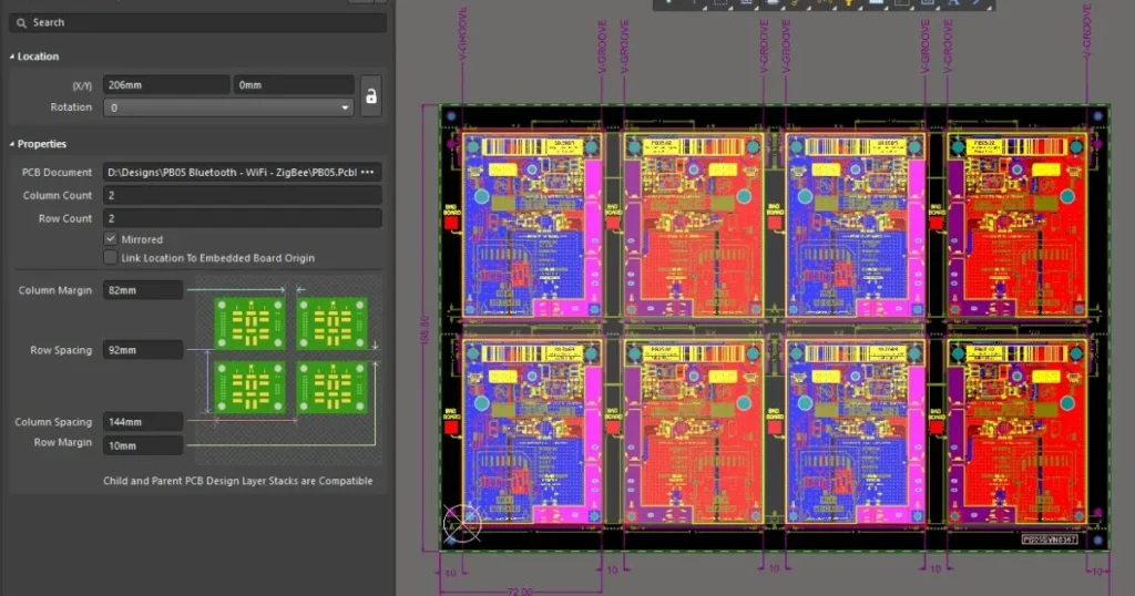
PCB panelization is the technique of arranging multiple individual boards into a larger composite panel, allowing for simultaneous processing during manufacturing. Instead of handling one PCB at a time, automated lines can handle entire panels, improving speed and accuracy.
This is especially crucial during SMT assembly, where pick and place machines require precise alignment and consistent board flow. Using fiducial marks, stencil alignment frames, and robust panel borders, panelization ensures seamless transitions between paste printing, component mounting, and reflow soldering.
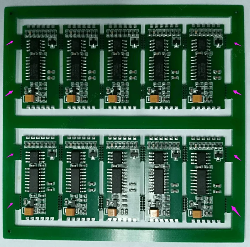
It also supports through-hole assembly and hybrid boards, where both SMT and THT components are used. By standardizing board orientation and spacing, panelization reduces misalignment, rework, and soldering inconsistencies.
PCB panelization allows manufacturers to process multiple boards simultaneously, improving throughput and reducing cost. Cadence offers a great breakdown of panelization basics.
How Does PCB Panelization Reduce Manufacturing Costs?
Panelization directly impacts production costs in several ways:
-
Reduced Setup Time: Loading a single panel with 4–12 boards is faster than loading individual PCBs.
-
Less Handling Labor: Fewer touchpoints mean fewer errors, especially during AOI inspection or manual soldering stages.
-
Material Efficiency: Optimized panel layout minimizes unused substrate space, reducing waste.
-
Faster Depaneling: Using V-cuts or breakaway tabs ensures boards can be separated quickly without damaging components.
These factors contribute to a more predictable cost structure, particularly for low-volume or prototype PCB panel assembly services, where every second counts.
What Are the Benefits of PCB Panelization?
PCB panelization for SMT offers more than just speed—it delivers consistency. This is critical for:
-
Double-sided SMT boards that require multiple reflow passes
-
Mixed technology assemblies (SMT + THT) where panel rigidity is essential. When using mixed SMT and through-hole components, panel design must prevent shadowing, misalignment, or solder bridging. These challenges are especially common in hybrid boards—this guide on combining SMT and THT offers practical solutions.
-
Low-volume production, where efficiency gains matter most
Panelization enables fast delivery PCB assembly with panelized boards, lowering lead times and increasing throughput. It also simplifies testing and quality control during the final stages of production.
If you’re sourcing from a one-stop PCB panel and post-soldering service, panelization ensures each part of the process—soldering, depaneling, inspection—is handled seamlessly without delays or rework.
Unit Circuits: Leading PCBA Manufacturer
 ISO-certified & 8+ years of PCBA Low MOQ & Fast Turnaround Prototype & Mass production
Limited Time Offer:
Get $100 off your order TODAY!
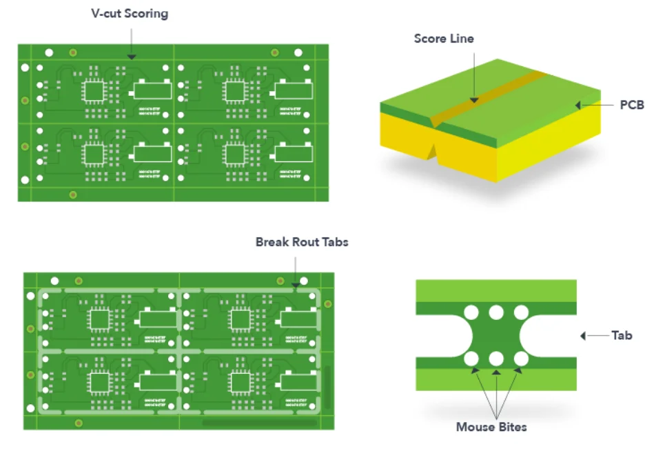
What Are Common Panelization Techniques?
There’s no one-size-fits-all approach. The right technique depends on your assembly needs:
V-Scoring (V-Groove)
Best for straight-edge boards. The panel is scored 1/3 depth from both sides and snapped apart post-assembly.
Tab-Routing (Breakaway Tabs)
Used for irregular shapes or complex outlines. Breakaway tabs include small perforations or mouse bites for easy depaneling.
Solid Panel with Custom Cutouts
Ideal for high-precision or heavy boards needing extra support during reflow or wave soldering.
Many defects during SMT or THT assembly stem from inconsistent handling, alignment errors, or soldering issues—all of which panelization can help minimize. For more on the root causes of production issues, see these common PCB assembly problems and solutions.
Choosing the correct PCB panel for THT soldering is crucial when wave soldering or manual post-assembly stages are involved. These methods must accommodate board warpage, fixture compatibility, and clearance for connectors.
Learn more about depaneling methods and fixture design in industry resources. Choosing between V-scores and mouse bites depends on your board shape and assembly method. Altium’s guide to depaneling methods explains the trade-offs in detail.
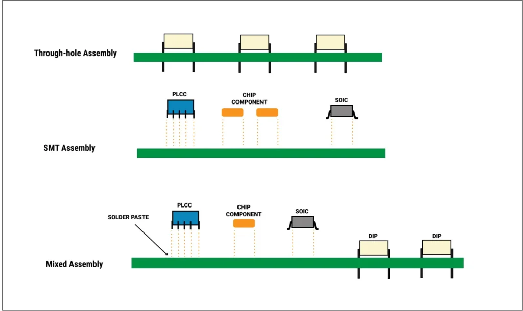
Panelized PCB for SMT and Through-Hole Assembly: What to Consider
Combining SMT and THT on one board presents challenges—double-sided soldering, connector clearance, and precise component height management.
Panelization solves these by allowing:
-
Proper spacing for tall through-hole parts
-
Clearance zones for manual soldering or wave soldering masks
-
Fixture-friendly layouts with added tooling holes and alignment guides
Panels must also support fiducial marks, pick-and-place orientation, and thermal balance during reflow. A poorly designed panel can lead to skewed parts, misaligned stencils, or thermal warping.
A good SMT PCB panel with THT connector assembly ensures your board survives both reflow and post-soldering stages without defect.
How to Panelize PCBs for Efficient SMT Production
Here are tips for effective SMT-ready panel design:
-
Consistent panel size (e.g. 250mm x 250mm) to fit standard stencil frames
-
Uniform component orientation to optimize pick and place path
-
1.6–3mm spacing between PCBs to prevent component damage during depaneling
-
Use of breakaway rails with fiducials, tooling holes, and barcodes for AOI
You’ll also want to consider DFM for panelized boards, especially if using lead-free soldering. The thermal profile must accommodate all parts without cold joints or bridging.
We recommend working with suppliers who offer panel optimization for manufacturing—not just panelization, but DFM feedback to ensure real-world production success.
Why Panelization Supports Small-Batch and Prototype Builds
For clients working in agile development, panelization is a lifesaver:
-
No need for costly NRE fees
-
Faster conversions between design iterations
-
Less downtime during assembly
Our low MOQ PCB panel assembly service is tailored for startups and innovators. We support both custom PCB panels for prototype and mass production, giving your team the flexibility to scale up without changing suppliers.
We also offer turnkey PCB panel service with component sourcing, giving you full support from Gerber upload to finished, tested boards—ready for enclosure.
PCB Delivery in Panels: What’s Best for Your Production Line?
Getting boards shipped in panels reduces the time your in-house team spends on prep and rework.
-
Assembly fixtures work better with standard panels
-
Wave soldering pallets need panel support
-
Post-solder inspection and functional test jigs rely on consistent layout
By choosing efficient PCB delivery with SMT-ready panel format, you simplify everything from receiving to final box build.
Ask your supplier if they offer DFM review and panel optimization as part of the quote. You’ll save time and reduce costly surprises.
FAQs
1. What’s the difference between a PCB and a panel?
A PCB is a single printed circuit board used in a device, while a PCB panel combines multiple PCBs on one larger board for efficient manufacturing. Panelization allows machines to assemble, solder, and test multiple units at once—ideal for SMT and through-hole assembly. Using panels reduces labor, speeds up production, and improves consistency in PCB assembly for electronics manufacturers.
2. Why choose PCBs over breadboard or manual wiring?
PCBs are far more reliable than breadboards or point-to-point wiring for any production-grade electronics. They ensure electrical integrity, reduce human error, and support automated SMT assembly. For manufacturers, panelized PCB solutions also speed up production, reduce defects, and support scalable testing—something manual wiring simply can’t offer.
3. What is panel plating in PCB manufacturing?
Panel plating is a process where the entire PCB panel is plated with a conductive material—typically copper—before patterning. It’s essential for creating robust vias and plated through-holes in double-sided and multilayer PCBs. This ensures strong electrical connectivity across layers, which is critical in SMT PCB panel designs that combine signal routing with power integrity.
4. Is PCB panelization suitable for low-volume production?
Yes—especially if you’re using a low MOQ PCB panel assembly service. Panelization minimizes cost even at low volumes by reducing setup time and labor. It’s ideal for prototype PCB panels, startups, and teams iterating quickly on designs. With fast delivery and turnkey PCB panel services, you get professional-grade results without large-batch commitments.
Have Specific Requirements?
Looking for high-precision PCB assembly for your products? Our team specializes in delivering top-tier assembly services, ensuring your devices perform flawlessly in any environment. Contact us today for a free consultation on how we can enhance your product’s reliability.
Summary
Proper panelization streamlines every stage of PCB assembly, reducing delays, defects, and cost. Ready to improve your next build? Upload your BOM file now—we’ll send back free DFM insights, optimized panel layout, and component sourcing options within 24 hours.
Upload your BOM file now for complimentary panelization recommendations + DFM review.
Get expert support for faster, more efficient assembly—no MOQ required, and results within 1 business day.
Save on your next PCB project?
Claim $100 OFF your order today.
✅ high-quality PCB assembly with strict quality control ✅ ISO-certified & 8+ years of experience. ✅ Low MOQ, fast turnaround, and 100% E-tested PCBs.
Additional Resources:
- How to Repair Circuit Boards: A Step-by-Step Beginner’s Guide
- Capacitor on Circuit Board: A Comprehensive Guide
- What Are PCB Conformal Coatings? Types, Benefits, and Applications Explained
- SMD Size Codes Explained: A Complete Guide to Understanding Surface-Mount Component Dimensions
- AC vs DC: Key Differences, Applications, and Advantages in Modern Electronics
Request for Quote
RECENT POSTS
IC Boards Explained: Applications, Layout Tips, and Assembly Services
Discover what IC boards are, how they’re used in modern electronics, and how to design
HDI PCB vs Multilayer PCB: How to Choose the Right One for Cost, Signal Integrity & Manufacturing
HDI PCB vs multilayer PCB explained from a manufacturing and assembly perspective. Learn how cost,
RELATED POSTS
Leading PCBA Manufacturer
✅ Assemble 20 PCBAS for $0 ✅ Get $100 OFF – Risk-Free Trial!
✅ 100+ Satisfied Customers
✅ Ensured Quality & On-Time Delivery
✅ Free Trial, No Commitments!