 Trusted by 100+ businesses worldwide No hidden fees – transparent pricing Guaranteed quality with on-time deliver
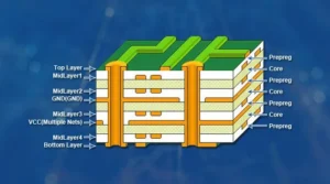
Multilayer PCB Signal Integrity: Expert Design Rules for Noise-Free Performance
Discover expert multilayer PCB signal integrity design rules and turnkey assembly solutions to ensure noise-free, high-speed performance—trusted by engineers needing precision and production reliability.
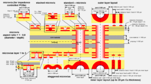
What is HDI PCB? | Ultimate Guide to Benefits, Structure, and Real-World Applications
Discover what HDI PCB is, how it works, and why our turnkey HDI PCB assembly delivers reliability, precision, and faster time-to-market.