Quick Leads-PCBA
🟢 Introduction: The Overlooked Key to Reliable IoT PCB Design
Smart home and industrial IoT devices are getting smaller, more powerful, and mass-produced at lightning speed. But there’s a hidden factor that determines their performance, durability, and manufacturability: PCB holes.
If you’re in high-volume PCB manufacturing, you’ve probably faced challenges like:
❌ Overheating in compact devices
❌ Weak electrical connections leading to failures
❌ Assembly defects that slow production
❌ Mechanical stress on fragile PCB components
Getting the hole design right solves these problems. Let’s break down why plated through-holes (PTH), vias, and mounting holes are non-negotiable for reliable, scalable PCB assembly. Learn more about PCB design.
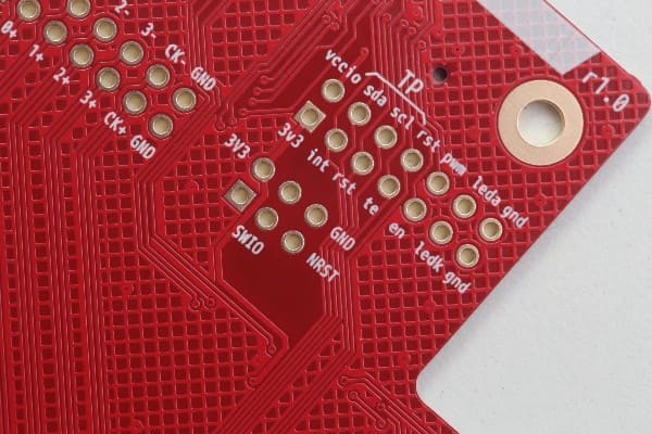
🟡 Why Do PCBs Have Holes?
PCB holes serve five critical functions:
✔ Electrical connections between layers (vias)
✔ Component mounting (mechanical strength)
✔ Thermal dissipation (reducing overheating)
✔ Signal integrity improvements (reducing interference)
✔ Automated assembly alignment (precision for mass production)
Without properly designed holes, a PCB can overheat, suffer connection failures, and be prone to mechanical damage—a major problem for IoT devices like Shelly’s smart thermostatic radiator valve (TRV).
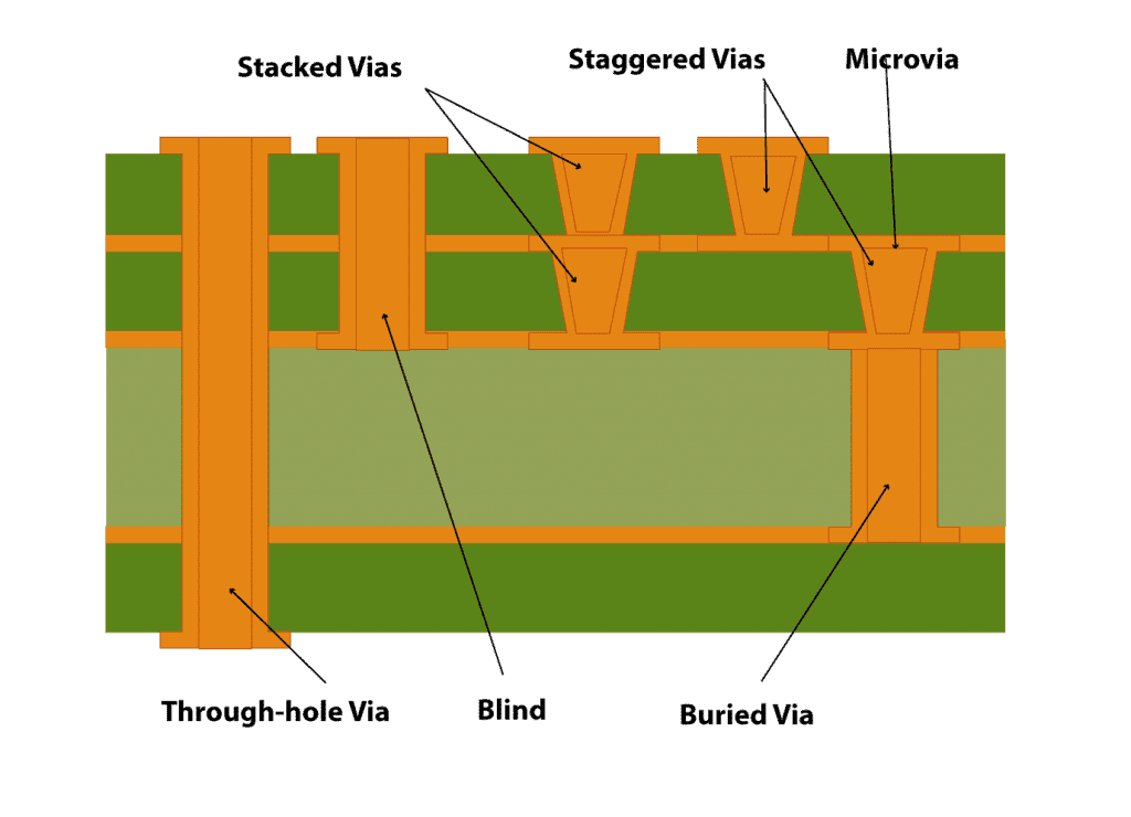
🔹 The Role of PCB Holes in High-Volume IoT Manufacturing
When producing millions of IoT devices like smart thermostats, sensors, and Wi-Fi-enabled controllers, even a tiny manufacturing defect can lead to thousands of faulty units.
Here’s a breakdown of common manufacturing pain points and how PCB holes solve them:
📊 Pain Points vs. PCB Hole Solutions
| Problem | Impact | Solution (Using PCB Holes) |
|---|---|---|
| Component Misalignment | Defective PCBs, high rejection rates | Tooling holes ensure precision alignment during assembly |
| Overheating in IoT Devices | Shortened lifespan, unstable performance | Thermal vias transfer heat away from sensitive components |
| Weak Solder Joints | Electrical failures over time | Plated through-holes reinforce mechanical strength |
| Signal Interference (EMI Issues) | Data loss, poor wireless performance | Shielding vias reduce EMI & maintain signal integrity |
Unit Circuits: Leading PCBA Manufacturer
 ISO-certified & 8+ years of PCBA
 Low MOQ & Fast Turnaround
 Prototype & Mass production
Limited Time Offer:
Get $100 off your order TODAY!
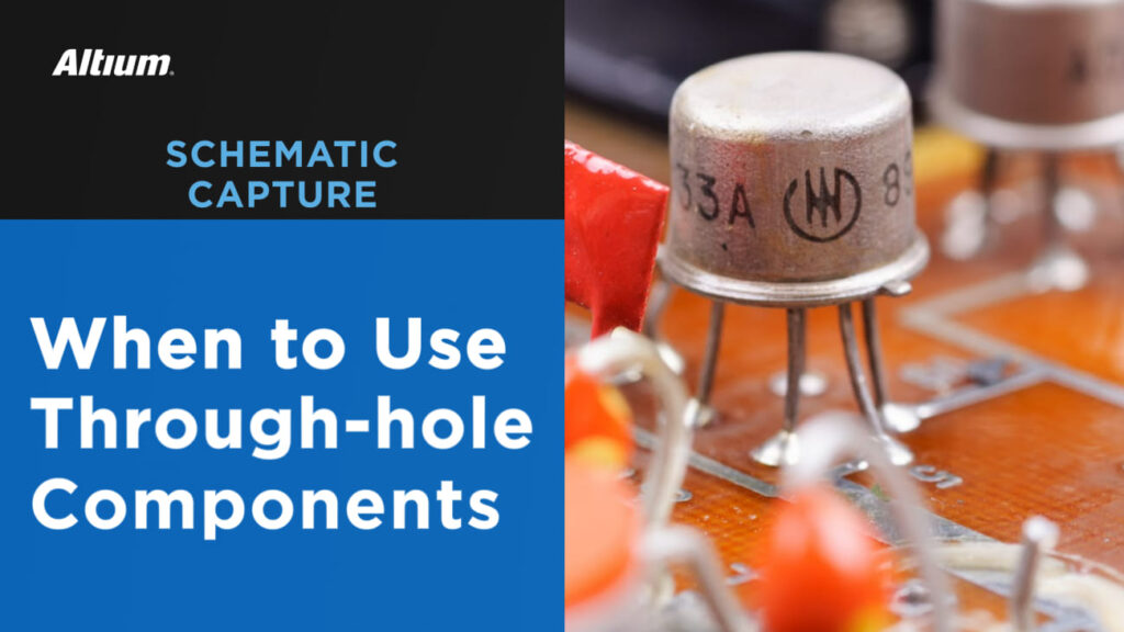
🔹 Electrical Connectivity Benefits of PCB Holes
🔍 How Plated Through-Holes Improve Reliability
PTH components are known for stronger solder connections because they’re anchored through the entire board. That means:
- Less risk of detachment under mechanical stress (important for industrial IoT applications)
- Higher current-carrying capacity for power components
- Better shock and vibration resistance
Plated through-holes (PTH) provide stronger solder joints and higher current-carrying capacity, making them ideal for high-reliability applications. Learn more about the benefits of plated through-hole technology in PCB design.
Ever wondered why critical components in industrial controllers often use PTH instead of SMT? It’s because PTH ensures a stronger, more reliable connection.
🔹 Mechanical Stability Advantages of PCB Holes
🔩 Why Mounting Holes Matter in IoT PCBs
- They prevent PCB cracking & warping (essential for high-temp applications like HVAC controllers)
- They absorb mechanical stress from connectors & fasteners
- They make it easy to secure PCBs inside enclosures without adhesives
Without mounting holes, a PCB relies entirely on solder joints for mechanical support—a huge risk in vibrating environments like automated HVAC systems.
🔹 Thermal Management: Why PCB Needs Holes for Heat Dissipation
🔥 The Problem: Heat Kills Electronics
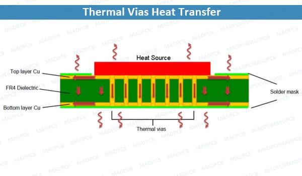
High-power IoT devices generate heat, and without proper heat dissipation, they’ll fail sooner than expected. Thermal vias solve this by:
✔ Moving heat from top layers to inner copper layers
✔ Connecting hot components to ground planes (heat spreaders)
✔ Reducing thermal stress on solder joints
For thermal management, via-in-pad technology and copper-filled vias are crucial for efficient heat dissipation. IPC’s research on via filling and through-hole plating explains how advanced plating processes improve heat conduction.
📌 Example: A smart radiator valve (TRV) needs efficient thermal vias near MOSFETs & voltage regulators. Without them, the PCB would overheat, reducing its lifespan.
🔹 Challenges in PCB Manufacturing & Solutions
🚨 Common Hole-Related Defects & How to Prevent Them
| Defect | What Causes It? | How to Prevent It? |
|---|---|---|
| Plating Voids | Poor copper deposition | Use high-quality electroless copper plating |
| Drill Wander | Misaligned drilling process | Laser-guided drilling for precision microvias |
| Copper Cracking | Thermal expansion stress | Use flexible copper plating techniques |
Through-hole assembly is still widely used in industrial and high-power PCBs due to its mechanical strength and durability. However, it requires precision drilling and plating to prevent defects. PCBWay provides a great breakdown of how through-hole assembly is optimized for modern manufacturing.
🔧 Best Practices for High-Volume IoT PCB Hole Design
1️⃣ Follow IPC-2221 standards for hole sizes
2️⃣ Use staggered microvias for high-density boards
3️⃣ Minimize drill hits to reduce production costs
FAQs
What are the consequences of misaligned PCB holes?
Misaligned holes cause assembly defects like:
❌ Components not fitting properly
❌ Solder joint failures
❌ Increased manufacturing rejects
Solution: Use tooling holes for precise hole placement during automated assembly.
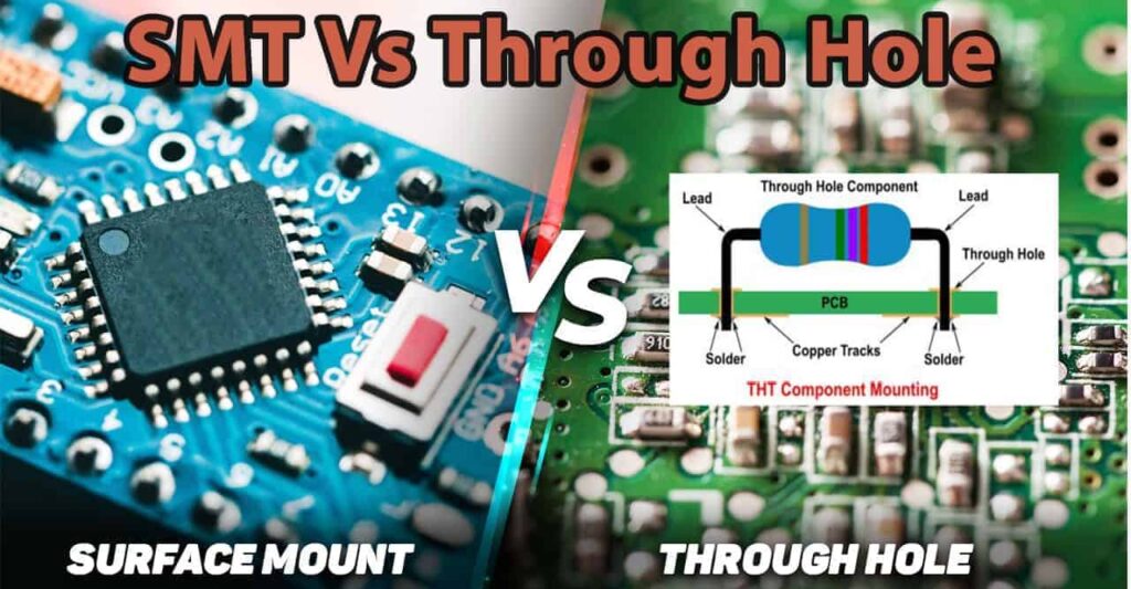
Are through-hole components still relevant in modern PCBs compared to SMT?
Yes! While SMT dominates, through-hole components are still essential for:
✔ High-power applications (better current capacity, e.g., up to 10A)
✔ Rugged IoT devices (stronger mechanical hold, ideal for vibration-prone environments)
✔ High-reliability industrial electronics(e.g., aerospace systems)
Unit Circuits offers both TH and SMT assembly for optimal design flexibility:SMT Assembly & TH Assembly
How do PCB holes affect signal integrity?
Poorly designed vias can cause signal reflections & EMI issues.
🔍 Solution: Use grounding vias & via stitching to reduce noise in high-frequency circuits.
Proper hole placement, size (e.g., 0.2mm-0.5mm for microvias), and shielding can minimize these effects. Our experts at Unit Circuits ensure optimal hole design for your PCB needs: PCB Manufacturing
How do PCB holes impact manufacturing costs?
💰 More drill hits = Higher costs
✔ Optimized hole placement reduces fabrication time
✔ Minimizing unnecessary via sizes lowers drilling costs
PCB holes increase costs due to drilling, plating, and inspection processes. Smaller holes (e.g., microvias) or higher densities raise expenses, but they improve performance. At Unit Circuits, we optimize hole designs to balance cost and quality, offering prototypes at $165 in 4 days.
Have Specific Requirements?
Looking for high-precision PCB assembly for your products? Our team specializes in delivering top-tier assembly services, ensuring your devices perform flawlessly in any environment. Contact us today for a free consultation on how we can enhance your product’s reliability.
🟢 Conclusion: Why Optimized PCB Holes Are Non-Negotiable
PCB holes are the backbone of reliable, high-performance IoT devices. Whether you’re designing smart home products, industrial controllers, or high-power electronics, optimizing hole placement will reduce failures, improve thermal efficiency, and enhance mass production scalability.
📢 🚀 Want a high-yield PCB assembly process? Get a free DFM analysis today!
Save on your next PCB project?
Claim $100 OFF your order today.
✅ high-quality PCB assembly with strict quality control ✅ ISO-certified & 8+ years of experience. ✅ Low MOQ, fast turnaround, and 100% E-tested PCBs.
Additional Resources:
- How to Repair Circuit Boards: A Step-by-Step Beginner’s Guide
- Capacitor on Circuit Board: A Comprehensive Guide
- What Are PCB Conformal Coatings? Types, Benefits, and Applications Explained
- SMD Size Codes Explained: A Complete Guide to Understanding Surface-Mount Component Dimensions
- AC vs DC: Key Differences, Applications, and Advantages in Modern Electronics
Request for Quote
RECENT POSTS
IC Boards Explained: Applications, Layout Tips, and Assembly Services
Discover what IC boards are, how they’re used in modern electronics, and how to design
HDI PCB vs Multilayer PCB: How to Choose the Right One for Cost, Signal Integrity & Manufacturing
HDI PCB vs multilayer PCB explained from a manufacturing and assembly perspective. Learn how cost,
RELATED POSTS
Leading PCBA Manufacturer
✅ Assemble 20 PCBAS for $0 ✅ Get $100 OFF – Risk-Free Trial!
✅ 100+ Satisfied Customers
✅ Ensured Quality & On-Time Delivery
✅ Free Trial, No Commitments!
