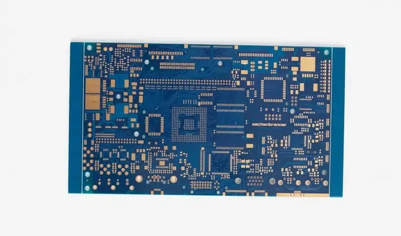
Quick Leads-PCBA
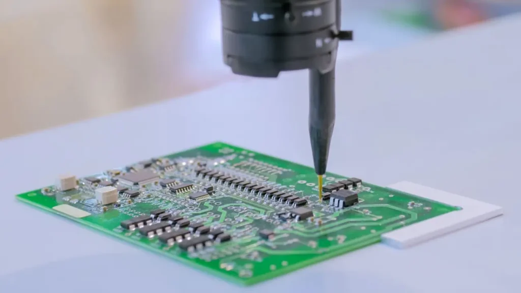
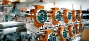
When sourcing PCB assembly services, one of the most common challenges engineers and decision-makers face is dealing with high Minimum Order Quantities (MOQ) and long lead times. These issues often complicate prototyping, small production runs, and product iterations, delaying progress. That’s where we come in. Our HDI PCB assembly services offer no MOQ requirements and fast delivery, ensuring you get exactly what you need, when you need it.
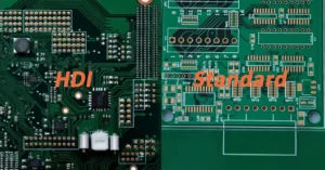
What is the Difference Between HDI PCB and Standard PCB?
Understanding the difference between HDI PCBs and standard PCBs is crucial when selecting the right technology for your project. While standard PCBs are still the backbone of most electronic devices, HDI (High-Density Interconnect) PCBs are designed to handle the ever-increasing demand for miniaturization and high-performance electronics.
Key Differences:
-
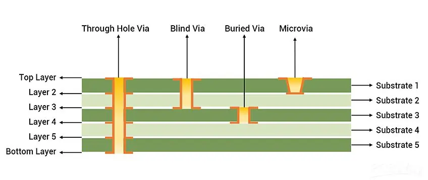
Micro-Vias: One of the main differentiators is the use of micro-vias in HDI PCB design. These are tiny holes drilled using laser technology, allowing for more complex layer stacking and greater electrical performance. In contrast, traditional PCBs use mechanical drilling, which limits design complexity.
-
Higher Layer Count: HDI PCBs can support more layers than standard PCBs, offering increased functionality in smaller packages. This is particularly important for applications where space is limited, such as mobile devices or IoT products.
-
Improved Performance: HDI boards are engineered to provide faster signal transmission speeds and improved electrical performance, especially in high-frequency applications.
For a comparison chart between HDI PCBs and standard PCBs, see below:
| Feature | HDI PCB | Standard PCB |
|---|---|---|
| Via Type | Laser-Drilled Micro-Vias | Mechanical Drilled Vias |
| Layer Count | Typically 6+ Layers | Usually 2-4 Layers |
| Signal Speed | High-Speed Transmission | Slower Signal Transmission |
| Application | High-Density, Miniaturized Devices | General Use in Larger Devices |
As you can see, HDI PCBs offer significant advantages in terms of design flexibility and electrical performance, making them ideal for cutting-edge products.One of the key advantages of HDI PCB is its reliability and performance, which is tested rigorously to meet industry standards.
To ensure these high standards, a variety of testing methods are used in the PCB assembly process. Learn more about these testing methods here to understand how HDI PCBs maintain their performance under different conditions.
What Are the Advantages of HDI PCB?
The benefits of using HDI PCBs are significant, especially when designing devices that require compact, high-performance circuits. Let’s break it down:
-
Compact Design: HDI PCBs enable designs with fewer components, reduced board sizes, and smaller geometries. This is a huge advantage in industries where space is at a premium, such as in wearable electronics or mobile devices.
-
Improved Electrical Performance: By using micro-via technology, HDI PCBs achieve faster data transmission speeds. This is especially beneficial for applications requiring high-frequency signal processing, such as 5G networks or automotive electronics.
-
Support for High-Density Components: HDI PCBs allow for more input/output (I/O) support in smaller board spaces. This is critical for developing high-performance, multi-functional devices without sacrificing performance or reliability. Reliability of CGA/LGA/HDI Package Board/Assembly
Unit Circuits: Leading PCBA Manufacturer
 ISO-certified & 8+ years of PCBA Low MOQ & Fast Turnaround Prototype & Mass production
Limited Time Offer:
Get $100 off your order TODAY!
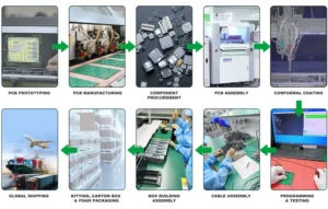
What Is the Difference Between PCB Assembly and PCB Manufacturing?
The terms PCB assembly and PCB manufacturing are often used interchangeably, but they refer to two distinct processes:
-
PCB Manufacturing: This is the process of creating the bare PCB, including the fabrication of the board itself, etching the copper traces, and drilling the holes.
-
PCB Assembly: This step comes after manufacturing. It involves placing and soldering the electronic components onto the board to create a fully functional circuit.
In Summary: While PCB manufacturing produces the physical board, PCB assembly focuses on integrating the components that make the board functional. At our facility, we offer a comprehensive service that includes both stages, making us your one-stop solution for custom PCB assembly needs.
In the process of HDI PCB assembly, it’s important to understand the difference between PCBs (Printed Circuit Boards) and PCBA (Printed Circuit Board Assemblies). This article dives into the nuances between the two, offering a clearer understanding of how HDI PCBs integrate into the assembly process.
What Is the Difference Between HDI and FR4?
FR4 is the most common base material used for standard PCBs, but when it comes to HDI PCBs, the material selection is slightly different due to the unique requirements of high-density interconnects.
-
FR4 is a rigid material made of glass fiber and epoxy resin, designed for standard PCBs. However, HDI PCBs require materials that are more flexible and can accommodate finer traces and more complex designs.
-
HDI Materials: HDI PCBs often use special materials such as polyimide or high-Tg FR4 that allow for denser layer stacking and improved thermal performance, particularly in high-frequency applications.
While FR4 remains the go-to for standard PCB designs, HDI materials provide the flexibility and performance needed for cutting-edge, high-density applications.
No MOQ HDI PCB Assembly Services: Why It Matters for Prototyping
One of the biggest frustrations in PCB manufacturing is the requirement for large minimum order quantities (MOQs). Traditionally, PCB suppliers have imposed high MOQs to make the manufacturing process cost-effective. However, this presents a problem for businesses that only need a small batch for prototyping or low-volume production.
Why Our No MOQ Service Is a Game Changer:
-
Cost-Effective Prototyping: No MOQ means that engineers and designers can order exactly what they need without worrying about waste or high upfront costs.
-
Faster Iterations: With no MOQ requirement, prototyping becomes faster. Engineers can quickly test, evaluate, and refine their designs, helping to accelerate time-to-market.
For example, in a typical no MOQ PCB assembly scenario, a design team can order only a handful of boards for testing, eliminating unnecessary overhead while ensuring that the product is tested under real-world conditions.
Sourcing HDI PCB assembly services with no MOQ and fast delivery is essential for many companies working on prototypes or small runs. This guide explains why choosing a reliable manufacturer in China for these services can be the perfect solution for businesses looking to minimize costs and accelerate production timelines.
Fast Turnaround HDI PCB Assembly: Meeting the Demands of the Electronics Industry
Time is often a critical factor in the electronics industry, particularly when it comes to getting products to market quickly. Whether you’re working on a quick-turn HDI PCB for a client or developing a prototype to showcase new technology, a fast turnaround time is crucial.
Here’s how our fast-turnaround HDI PCB assembly works:
-
Expedited Manufacturing: We prioritize speed in every stage, from fabrication to assembly, ensuring your boards are ready in record time.
-
Same-Day PCB Assembly: For urgent projects, we can complete custom HDI PCB assemblies within 24-48 hours, providing you with the rapid prototyping service you need.
By offering quick-turn HDI PCB assembly, we help you meet tight deadlines without compromising on quality.
How Custom HDI PCB Assembly Solutions Solve Complex Engineering Challenges
When it comes to advanced electronics, one-size-fits-all solutions don’t always work. That’s where custom HDI PCB assembly solutions come in. Whether you’re designing a wearable device or a high-performance automotive system, we can tailor our services to meet your specific needs.
-
Tailored Designs: We work with you to create PCBs that match your exact design specifications, ensuring the final product performs exactly as intended.
-
Advanced Prototyping: We specialize in HDI PCB assembly for prototyping, helping engineers test new concepts and refine designs before committing to full production.
FAQs
1. What Is an HDI PCB?
HDI PCB (High-Density Interconnect PCB) refers to a type of printed circuit board designed with micro-vias, blind vias, and buried vias. These features enable higher circuit density and better electrical performance in compact designs. HDI PCBs are ideal for applications requiring faster signal transmission and miniaturization, such as mobile devices, IoT products, and wearable electronics. The use of advanced materials in HDI PCB assembly allows for more layers and finer traces compared to standard PCBs, making them suitable for high-performance applications.
2. What Is the Difference Between HDI and E HDI?
E HDI (Enhanced High-Density Interconnect) is an advanced form of HDI PCB. While both feature micro-via technology for high-density designs, E HDI offers even smaller via sizes and higher layer counts, providing increased performance for more complex applications. E HDI PCBs are often used in cutting-edge technologies like 5G networks and high-end consumer electronics, where fast data transmission and space-saving designs are essential. If you need advanced features like rapid prototyping with custom HDI PCB assembly solutions, E HDI might be the ideal choice.
3. Why is FR4 Used in PCB?
FR4 is the most common material used in PCB manufacturing because of its excellent combination of electrical insulating properties, durability, and affordability. It's a type of fiberglass-reinforced epoxy material that's ideal for standard PCBs. FR4 is widely used in a variety of electronics due to its ability to withstand high temperatures and its cost-effectiveness. However, for high-density interconnect (HDI PCBs), FR4 has limitations in accommodating fine traces and high-frequency signals, which is why HDI materials are preferred in more advanced designs.
4. What is the Difference Between IMS and FR4 PCB?
IMS (Insulated Metal Substrate) and FR4 are both materials used in PCB manufacturing, but they serve different purposes. IMS PCBs use a metal base, typically aluminum, to enhance heat dissipation, making them ideal for applications with high power requirements, such as LED lighting and power electronics. On the other hand, FR4 PCBs are made from fiberglass and epoxy resin, offering superior electrical insulation for general-purpose applications. If your design involves high power dissipation, IMS PCBs might be a better choice, while FR4 is suitable for more standard projects.
Have Specific Requirements?
Looking for high-precision PCB assembly for your products? Our team specializes in delivering top-tier assembly services, ensuring your devices perform flawlessly in any environment. Contact us today for a free consultation on how we can enhance your product’s reliability.
Summary
In conclusion, HDI PCB assembly is a game-changer for engineers and businesses looking to push the boundaries of innovation. By eliminating the burden of high MOQ requirements and offering fast delivery, we make it easier to prototype, iterate, and launch new products quickly. Whether you’re looking for custom HDI PCB assembly solutions or a fast turnaround service, we have you covered.
Let’s work together to accelerate your project’s timeline and take your designs to the next level.
Save on your next PCB project?
Claim $100 OFF your order today.
✅ high-quality PCB assembly with strict quality control ✅ ISO-certified & 8+ years of experience. ✅ Low MOQ, fast turnaround, and 100% E-tested PCBs.
Additional Resources:
- How to Repair Circuit Boards: A Step-by-Step Beginner’s Guide
- Capacitor on Circuit Board: A Comprehensive Guide
- What Are PCB Conformal Coatings? Types, Benefits, and Applications Explained
- SMD Size Codes Explained: A Complete Guide to Understanding Surface-Mount Component Dimensions
- AC vs DC: Key Differences, Applications, and Advantages in Modern Electronics
Request for Quote
RECENT POSTS
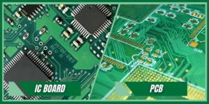
IC Boards Explained: Applications, Layout Tips, and Assembly Services
Discover what IC boards are, how they’re used in modern electronics, and how to design
HDI PCB vs Multilayer PCB: How to Choose the Right One for Cost, Signal Integrity & Manufacturing
HDI PCB vs multilayer PCB explained from a manufacturing and assembly perspective. Learn how cost,
RELATED POSTS
Leading PCBA Manufacturer
✅ Assemble 20 PCBAS for $0 ✅ Get $100 OFF – Risk-Free Trial!
✅ 100+ Satisfied Customers
✅ Ensured Quality & On-Time Delivery
✅ Free Trial, No Commitments!