
Last Updated: September 18, 2026
The five common PCB assembly testing methods are in-circuit testing (ICT), flying probe testing, automated optical inspection (AOI), X-ray inspection, and functional testing (FCT). They detect different types of assembly defects, so the right method depends on board complexity, production volume, test coverage, and whether you need to verify manufacturing defects or actual board functions.
For prototypes and low-volume PCB assembly, flying probe testing is often practical because it does not require a dedicated test fixture. ICT is better suited to repeatable higher-volume testing, while AOI and X-ray inspection identify visible or hidden assembly defects. Functional testing verifies whether the assembled PCB performs its intended functions.
Why PCB Assembly Testing Requires More Than One Method
No single PCB testing method detects every type of defect. A practical PCB test strategy combines inspection and electrical or functional testing based on the board design, production stage, volume, and required test coverage.
AOI and X-ray inspection are used to identify assembly defects, while ICT and flying probe testing check electrical connections and component-related faults. Functional testing serves a different purpose: it verifies whether the assembled board performs its specified functions. The appropriate combination depends on the risks and requirements of each PCBA project.
Quick Leads
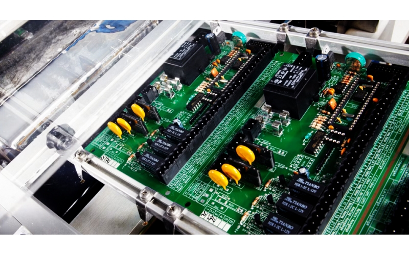
1. Why is In-Circuit Testing (ICT) Essential for PCB Quality?
Benefits:
- Broad electrical fault coverage: Can detect many assembly-related faults, including opens, shorts, and component-related errors.
- Fast and repeatable: Ideal for mass production.
- Comprehensive testing: Detects open circuits, shorts, and soldering issues.
Best Applications:
- High-volume or repeat production where the PCB design is stable and fast, repeatable testing is required.
Challenges:
- Fixture cost: A dedicated ICT fixture adds upfront cost, making ICT less attractive for prototypes or frequently changing designs.
- Limited flexibility: PCB design or test-point changes may require fixture modification or replacement.
Example:
2. When Should You Use Flying Probe Testing (FPT) in PCB Assembly?
Benefits:
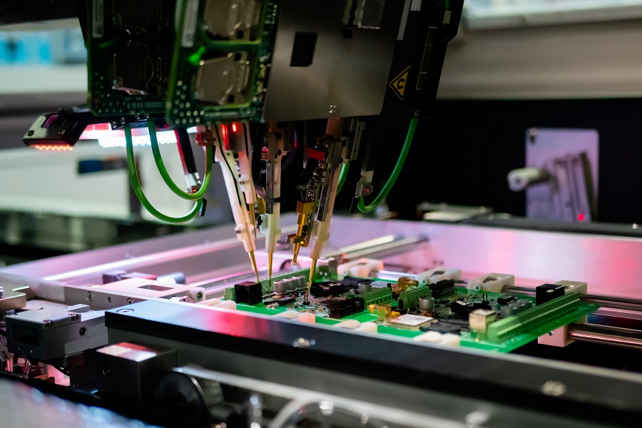
- No dedicated fixture: Reduces upfront tooling requirements compared with ICT.
- Flexible for design changes: Test programs can be adjusted when the PCB design is revised.
- Suitable for low-volume builds: Useful for prototypes and smaller production runs where a dedicated ICT fixture may not be economical.
Best Applications:
- Prototypes, low-volume production, and PCB projects with frequent design revisions.
Challenges:
- Test access limitations: Dense layouts, very small test points, or limited probe access can restrict test coverage.
- Slower test cycle: Because probes move between test points, flying probe testing is generally slower than fixture-based ICT for higher-volume production.
3. How Does Automated Optical Inspection (AOI) Improve PCB Quality?
Benefits:
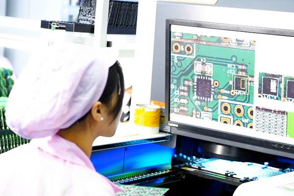
- Fast, non-contact inspection: AOI can inspect assembled boards without physically probing test points.
- Detects visible assembly defects: Identifies issues such as missing components, placement errors, polarity problems, and solder defects that are visible to the inspection system.
- Suitable for production inspection: AOI can be integrated into PCB assembly workflows to identify defects before later testing stages.
Best Applications:
- PCB assembly inspection where visible component placement and soldering defects need to be identified during production.
Challenges:
- Limited to visible features: AOI cannot directly inspect hidden solder joints underneath components such as BGAs.
- Programming and inspection criteria matter: Inspection results depend on the system setup, board design, and defined acceptance criteria.
4. Why Use X-Ray Inspection for High-Density PCBs?
Benefits:
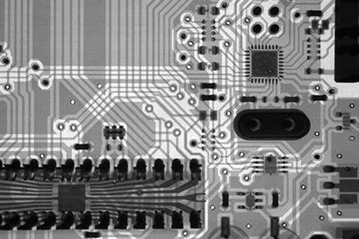
- Detects hidden assembly defects: Allows inspection of solder joints underneath components such as BGAs and QFNs.
- Supports complex PCB assemblies: Useful where component packages or board layouts make visual inspection insufficient.
- Complements AOI: X-ray inspection can evaluate hidden features that optical inspection cannot directly see.
Best Applications:
- PCB assemblies with BGAs, QFNs, or other components where critical solder joints are hidden from optical inspection.
Challenges:
- Higher inspection cost: X-ray equipment and operation generally involve higher costs than optical inspection.
- Requires interpretation: X-ray images must be evaluated using appropriate inspection criteria and experienced judgment.
Example:
5. What is Functional Testing (FCT) in PCB Manufacturing?
Benefits:
- Verifies board-level functions: Confirms whether the assembled PCB performs the functions defined in the test requirements.
- Project-specific testing: Test procedures, fixtures, equipment, and acceptance criteria can be configured around the requirements of the product.
Best Applications:
- Final functional verification when specified board-level operation must be confirmed before shipment or integration into the finished product.
Challenges:
- Requires project-specific setup: Fixtures, test programs, equipment, and procedures may need to be developed for a specific PCBA.
- Test time affects throughput: More extensive functional test procedures can increase the test time per board.
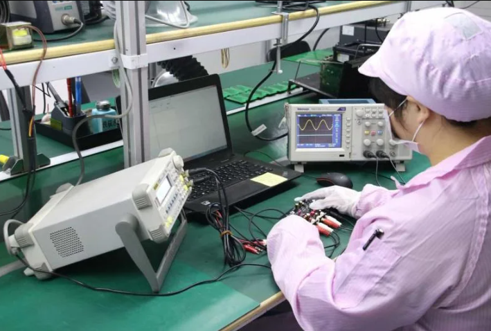
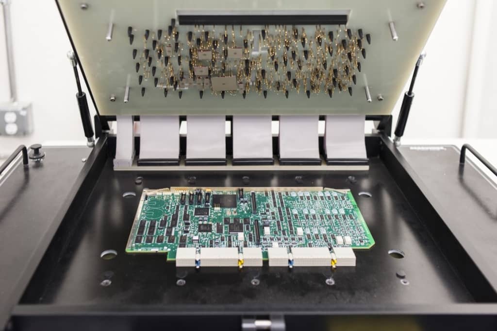
Comparison of PCB Testing Methods
| Method | What It Checks | Best For | Main Advantage | Main Limitation |
|---|---|---|---|---|
| In-Circuit Testing (ICT) | Electrical connections and component-related faults | Stable designs and higher-volume production | Fast, repeatable testing with dedicated fixtures | Requires fixture investment and test access |
| Flying Probe Testing | Electrical connections and selected component parameters | Prototypes, low-volume builds, and changing designs | No dedicated bed-of-nails fixture required | Slower than ICT for higher-volume testing |
| Automated Optical Inspection (AOI) | Visible component placement and soldering defects | Production-stage visual inspection | Fast, non-contact inspection of visible defects | Cannot directly inspect hidden solder joints |
| X-Ray Inspection | Hidden solder joints and internal assembly features | BGAs, QFNs, and assemblies with hidden connections | Detects defects that optical inspection cannot see | Higher inspection cost and requires image interpretation |
| Functional Testing (FCT) | Specified board-level functions | Final functional verification | Confirms whether the assembled PCB performs required functions | Requires project-specific test setup and procedures |
In practice, PCB assembly testing often combines multiple methods rather than relying on a single test. The appropriate test strategy depends on board design, production volume, defect risks, test access, and required functional coverage.
How to Choose a PCB Testing Method for Your Project
Choosing a PCB testing method starts with the defects and risks you need to detect, not with selecting a single “best” test. Consider the PCB design, component types, test-point accessibility, production volume, expected design changes, and required functional coverage.
For many PCB assembly projects, the appropriate test strategy combines inspection with electrical or functional testing. Prototype and low-volume builds may prioritize flexibility, while stable production runs may justify dedicated test fixtures. Boards with hidden solder joints may also require X-ray inspection, while functional testing is appropriate when specified board-level operation must be verified.
Need PCB Assembly and Testing Support?
Send us your PCB files, BOM, production quantity, and testing requirements. We can review the project and recommend an appropriate assembly and testing approach based on your board and production needs.
Request for Quote
RECENT POSTS
What Are PCB Silkscreen Design Guidelines? (Clearance, Font Size & DFM Rules Explained)
Learn PCB silkscreen design guidelines, including font size, clearance, and DFM rules. Improve readability, prevent
What Is PCB Silkscreen Used For? Functions, Symbols & Practical Examples
Learn what PCB silkscreen is used for, including symbols, functions, and real applications. Improve assembly
RELATED POSTS
Leading PCBA Manufacturer
✅ Assemble 20 PCBAS for $0 ✅ Get $100 OFF – Risk-Free Trial!
✅ 100+ Satisfied Customers
✅ Ensured Quality & On-Time Delivery
✅ Free Trial, No Commitments!

 Assemble 20 PCBAS for $0