Quick Leads-PCBA
 Looking for full-service PCB Assembly?
Turnkey solutions from PCB manufacturing to testing.
sales@unitcircuits.com
Introduction
Shrinking device sizes, increasing functionality, and the need for faster signal transmission are pushing engineers to rethink PCB design. Yet many decision-makers struggle with sourcing HDI PCB assembly services that align with their real-world engineering and procurement challenges. Let’s break down what HDI PCBs are—and why getting both the design and assembly right is critical.
What is an HDI PCB?
High Density Interconnect (HDI) PCBs are multilayer circuit boards with densely packed routing, using microvias, blind and buried vias, and advanced lamination techniques. They’re designed for applications requiring compact size, high-speed signal transmission, and reliable performance. HDI PCB manufacturing involves precision fabrication and assembly, often supported by turnkey solutions to streamline development.
Now let’s dive deeper into how HDI PCBs are structured, manufactured, and why choosing the right partner directly impacts your project’s success.
What Does HDI Mean in PCB Design?
HDI, or High Density Interconnect, refers to a PCB design methodology that enables significantly higher wiring density per square inch compared to conventional PCBs. This is achieved through:
-
Microvias: Ultra-small vias for layer-to-layer connections.
-
Blind Vias: Connect outer layers to inner layers without going through the entire board.
-
Buried Vias: Connect internal layers, hidden from the surface.
-
Via-in-Pad: Allows direct component placement on vias for reduced signal path and better performance.
These structures enable a tighter PCB stack-up, essential for today’s fine-pitch components and BGA packages.
What Does HDI PCB Mean?
HDI PCBs represent a class of printed circuit boards that offer:
-
Higher component density
-
Reduced layer count with enhanced performance
-
Optimized signal integrity
-
Smaller footprints without sacrificing function
For example, medical wearables, automotive radar modules, and IoT devices all depend on HDI layouts to meet strict space and performance constraints.
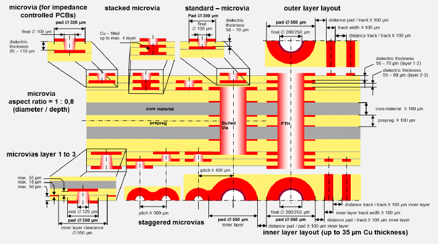
HDI PCB design involves blind, buried, and microvias, along with fine trace widths. Altium’s guide on HDI design basics offers a helpful technical breakdown for engineers new to these concepts.
What is the HDI Process of PCB?
The HDI manufacturing process includes:
-
Inner Layer Etching – Copper foils patterned for signal routing.
-
Sequential Lamination – Alternating layers of core and prepreg laminated under heat and pressure.
-
Drilling Microvias – Laser drilling for sub-150μm vias.
-
Copper Plating – Ensures conductivity through blind/buried vias.
-
Impedance Control – Ensures high-speed signal integrity.
-
Surface Finish & Solder Mask – RoHS-compliant finishes like ENIG or HASL.
-
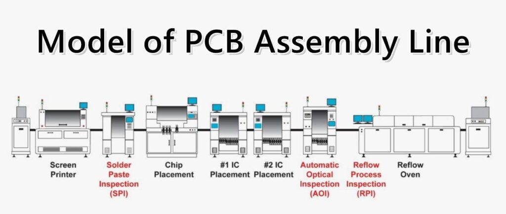
SMT Assembly – Placement and soldering of fine-pitch components using reflow soldering.
Every step must maintain ±25μm alignment precision, especially with via-in-pad and BGA designs.
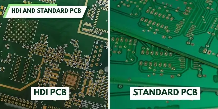
What is the Difference Between HDI PCB and Normal PCB?
| Feature | Standard PCB | HDI PCB |
|---|---|---|
| Layer Count | 2–6 layers | 4–16+ layers |
| Vias | Through-hole only | Blind, buried, microvias, via-in-pad |
| Routing Density | Low | Very high |
| Size Efficiency | Lower | 30–50% space-saving |
| Cost per Unit | Lower | Higher, but optimized per function |
| Ideal Use Cases | Consumer electronics | Automotive, medical, industrial, IoT |
HDI PCBs aren’t simply “smaller”—they are designed for more demanding applications, requiring tight impedance control, complex stack-ups, and advanced testing protocols.
Unit Circuits: Leading PCBA Manufacturer
 ISO-certified & 8+ years of PCBA Low MOQ & Fast Turnaround Prototype & Mass production
Limited Time Offer:
Get $100 off your order TODAY!
sales@unitcircuits.com
Why HDI PCB Projects Fail: 5 Hidden Risks to Avoid
1. High Entry Costs & MOQ Restrictions
Many suppliers enforce rigid MOQs, making early prototyping costly.
But HDI development is iterative—it starts with low-volume:
-
Proof-of-concept prototypes
-
Engineering validation builds
-
Functional pilot runs
✅ Our Solution: We offer HDI PCB turnkey assembly starting from low-volume runs—bridging R&D to mass production with no MOQ bottlenecks.
Many engineers struggle with rigid MOQ policies when trying to validate HDI designs. For fast prototyping and pilot builds, choosing an HDI PCB manufacturer that offers no-MOQ turnkey assembly solutions can accelerate development without sacrificing quality.
2. Fragmented Supply Chains
Typical process:
-
One vendor for HDI PCB fabrication
-
Another for SMT assembly
-
Another for testing and rework
This causes:
-
Lead time inflation
-
Miscommunication
-
DFM/DFA mismatches
✅ Our Solution: A one-stop HDI PCB solution for engineers—from fabrication to functional testing under a single ISO-compliant system.
3. Quality and Reliability Risks in Assembly
HDI designs are unforgiving:
-
Misplaced microvias → short/open circuits
-
Poor BGA soldering → intermittent faults
-
Inadequate testing → field failures
Cheap providers lack:
-
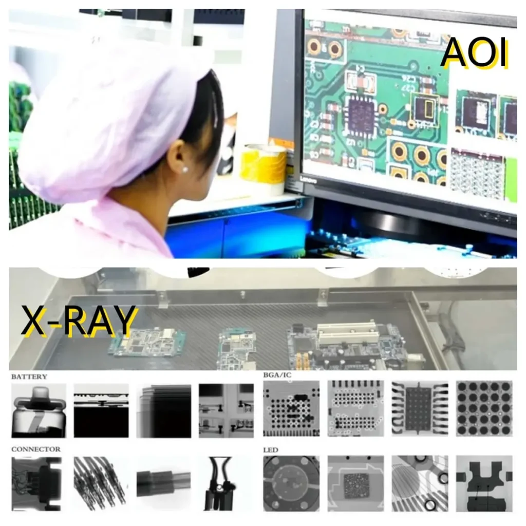
AOI, ICT, and functional testing
-
RoHS compliance tracking
-
Traceability across batches
✅ Our Solution: Full-stack assembly with HDI PCB with testing and inspection, including reflow profiles, BGA x-ray, and IPC Class 2/3 certifications.
4. DFM Gaps During Design Transition
Common engineer pain points:
-
Incorrect stack-up design
-
Improper via-in-pad routing
-
Poor thermal relief planning
-
Mismatched impedance lines
✅ Our Solution: Early-stage DFM checks with Gerber reviews and stack-up simulation. We assist with impedance tuning, thermal management, and DFM for HDI PCB.
5. Misaligned Sourcing on Ultra-Low-Cost Platforms
Platforms like JLCPCB are fine for hobbyists. But for real-world HDI applications, their limitations are clear:
-
Inconsistent soldering quality
-
Lack of fine-pitch support
-
No functional testing
-
No accountability
✅ Our Position: We do not serve hobbyist or low-budget buyers. Our services are tailored for OEMs, engineers, and system integrators who prioritize reliability and precision.
HDI PCB Stack-Up and Design Rules
We assist clients with:
-
Balanced multilayer stack-up design
-
Proper copper thickness and prepreg selection
-
Controlled impedance routing
-
Thermal relief pad layout
-
Design compliant with IPC-2226 and IPC-6012 standards
🧠 Bonus: Request our HDI PCB Design Guide PDF for optimized layouts.
SMT Assembly for HDI PCBs: How We Solve Real-World Issues
HDI SMT assembly demands:
-
BGA and fine-pitch placement (down to 0.3mm pitch)
-
Reflow soldering profiles tailored per board
-
X-ray inspection for hidden joints
We support:
-
HDI PCB with SMT service
-
One-stop electronics manufacturing
-
Custom HDI PCB for industrial use
Why Functional Testing is Non-Negotiable
Testing is not an option—it’s the final gate.
Our HDI testing suite includes:
-
AOI (Automated Optical Inspection)
-
ICT (In-Circuit Testing)
-
FCT (Functional Circuit Testing)
-
Environmental and thermal cycling (on request)
✅ 100% traceable reports. ✅ RoHS and REACH compliance.
A strong HDI PCB process doesn’t end at soldering. Comprehensive testing—including ICT, AOI, and functional checks—is essential. These top testing methods for high-quality PCB assembly ensure early detection of faults before integration.
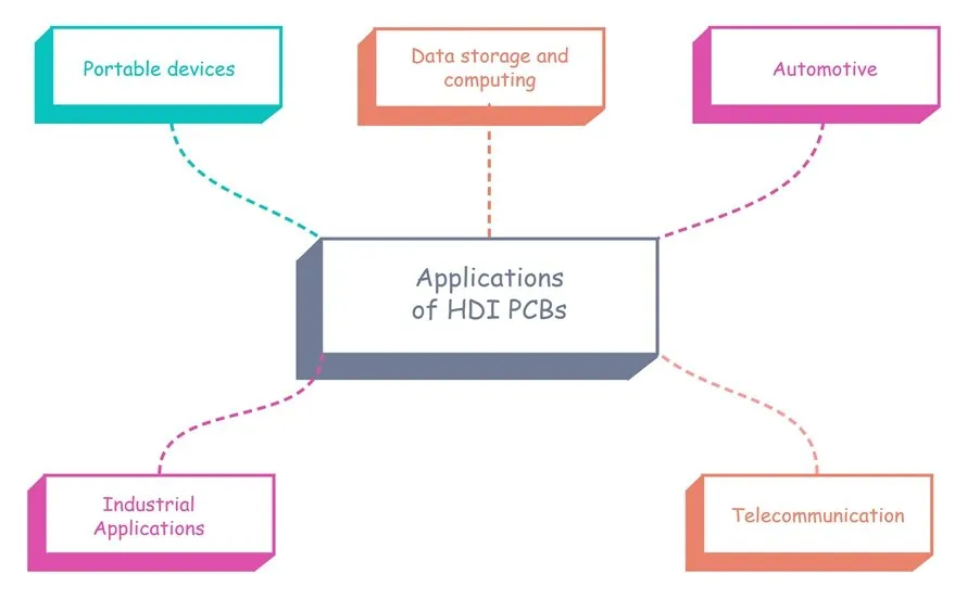
HDI PCB Applications in Smart Devices and Automation
Use cases we serve:
-
HDI PCB for medical devices
-
HDI PCB for automotive radar systems
-
High-density PCB for IoT and automation equipment
-
HDI PCB assembly for smart devices
HDI unlocks power + performance in limited space.
Scalable HDI PCB Manufacturing for OEMs
We specialize in:
-
Multilayer HDI PCB manufacturing China-based
-
Low-volume → high-volume scalability
-
Fast delivery HDI PCB with components pre-sourced
-
Engineering flexibility + stable pricing for repeat orders
How to Choose the Right HDI PCB Partner
When sourcing, ask:
-
Can they do both fabrication + assembly under one roof?
-
Do they support via-in-pad and microvia structures?
-
Can they do RoHS, IPC Class 3, and full traceability?
-
Are functional tests standard, not optional?
Avoid “low-price only” options. Focus on long-term supply partnerships that scale with your roadmap.
FAQs
1. What makes your HDI PCB turnkey assembly different from other providers?
Our HDI PCB turnkey assembly service integrates fabrication, SMT placement, component sourcing, and final testing in a single, traceable workflow. Unlike fragmented vendors, we ensure alignment from CAD to shipment, reducing lead times and costly rework. This one-stop approach is ideal for OEMs needing reliable, fast delivery HDI PCBs with components—not DIY-level service.
2. Can I get a custom HDI PCB prototype with professional testing?
Yes. We support custom HDI PCB prototype assembly with full testing, including AOI, ICT, and functional validation. Our process meets IPC standards for HDI, ensuring your prototype reflects production-level quality. This helps engineers validate designs quickly and accurately—without sacrificing reliability.
3. Do you support HDI PCB assembly for industrial and IoT applications?
Absolutely. We specialize in HDI PCB for industrial use, including high-density PCB for IoT and automation systems. Our engineers work with you on stack-up design, thermal management, and impedance control, ensuring durability in harsh or high-frequency environments. We optimize for long-term performance, not just unit cost.
4. How do you ensure fine-pitch SMT placement is accurate on HDI PCBs?
We use high-precision SMT lines calibrated for BGA and fine-pitch placement as small as 0.3mm. Coupled with via-in-pad designs and controlled reflow soldering, we minimize tombstoning and solder bridging. Our DFM for HDI PCB review ensures your layout is optimized for yield before production starts.
Have Specific Requirements?
Looking for high-precision PCB assembly for your products? Our team specializes in delivering top-tier assembly services, ensuring your devices perform flawlessly in any environment. Contact us today for a free consultation on how we can enhance your product’s reliability.
Summary
Choosing the right HDI PCB partner means balancing innovation with reliability. We offer custom, fully tested solutions for OEMs, engineers, and product developers.
Ready to build smaller, faster, and smarter? Request a quote or free engineering consultation →
Save on your next PCB project?
Claim $100 OFF your order today.
sales@unitcircuits.com
✅ high-quality PCB assembly with strict quality control ✅ ISO-certified & 8+ years of experience. ✅ Low MOQ, fast turnaround, and 100% E-tested PCBs.
Additional Resources:
- How to Repair Circuit Boards: A Step-by-Step Beginner’s Guide
- Capacitor on Circuit Board: A Comprehensive Guide
- What Are PCB Conformal Coatings? Types, Benefits, and Applications Explained
- SMD Size Codes Explained: A Complete Guide to Understanding Surface-Mount Component Dimensions
- AC vs DC: Key Differences, Applications, and Advantages in Modern Electronics
Request for Quote
sales@unitcircuits.com
RECENT POSTS
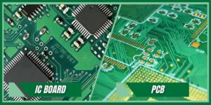
IC Boards Explained: Applications, Layout Tips, and Assembly Services
Discover what IC boards are, how they’re used in modern electronics, and how to design
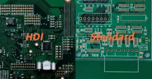
HDI PCB vs Multilayer PCB: How to Choose the Right One for Cost, Signal Integrity & Manufacturing
HDI PCB vs multilayer PCB explained from a manufacturing and assembly perspective. Learn how cost,
RELATED POSTS
Leading PCBA Manufacturer
✅ Assemble 20 PCBAS for $0 ✅ Get $100 OFF – Risk-Free Trial!
sales@unitcircuits.com
✅ 100+ Satisfied Customers
✅ Ensured Quality & On-Time Delivery
✅ Free Trial, No Commitments!