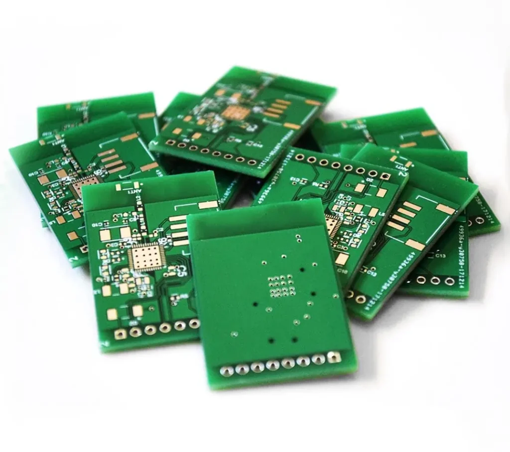
Quick Leads-PCBA
Printed Circuit Board (PCB) thickness isn’t just a number—it directly affects performance, durability, and manufacturing costs. Get it wrong, and you might end up with overheating issues, signal integrity problems, or even mechanical failure.
So, how do you choose the right PCB thickness for your design? This guide breaks it down into five key factors that every engineer, designer, and decision-maker should consider. Plus, we’ll explore industry challenges and real-world solutions to ensure you get the most efficient, cost-effective PCB thickness for your needs.
1. What Is PCB Thickness & Why Does It Matter?
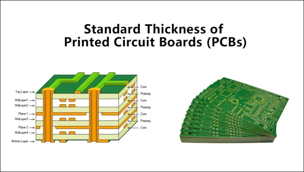
PCB thickness refers to the overall height of a printed circuit board, measured in millimeters (mm) or mils (thousandths of an inch). Standard PCBs typically range from 0.2 mm (8 mils) to 6.0 mm (236 mils), with 1.57 mm (62 mils) being the most common.
Why does thickness matter? It impacts:
- Signal integrity (thicker boards may require impedance matching)
- Heat dissipation (thinner boards heat up faster)
- Mechanical durability (flexibility vs. rigidity)
- Manufacturing constraints (cost and lead time considerations)
📌 Quick Fact: Most consumer electronics use a 1.57mm PCB because it balances cost, performance, and manufacturability.
Selecting the right PCB thickness is crucial for performance and reliability. Factors like material choice, mechanical strength, and electrical requirements all play a role. For a detailed breakdown of industry standards and best practices, check out this comprehensive guide from JLCPCB.
2. The 5 Key Factors in Choosing PCB Thickness
1️⃣ Electrical Performance: Signal Integrity & Impedance Control
For high-speed and RF circuits, PCB thickness affects impedance matching and signal integrity. A thinner PCB reduces parasitic capacitance but may also increase crosstalk.
💡 Best PCB Thickness for Signal Integrity:
- High-frequency RF & microwave applications: 0.8mm to 1.2mm
- Standard digital circuits: 1.57mm
- High-power applications: 2.36mm or more
Tip: When working with high-speed signals, always match PCB thickness with controlled impedance requirements.
Unit Circuits: Leading PCBA Manufacturer
 ISO-certified & 8+ years of PCBA Low MOQ & Fast Turnaround Prototype & Mass production
Limited Time Offer:
Get $100 off your order TODAY!
2️⃣ Thermal Management & Heat Dissipation
A thicker PCB generally helps with heat dissipation, especially in power electronics. However, too much thickness can lead to poor thermal cycling resistance and higher material costs.
💡 How PCB Thickness Affects Heat Dissipation:
- Thin PCBs (<1.0mm): Poor heat dissipation, suitable for low-power devices
- Medium PCBs (1.57mm): Standard balance between thermal and mechanical properties
- Thick PCBs (>2.36mm): Good for power electronics, but may need additional heat sinks
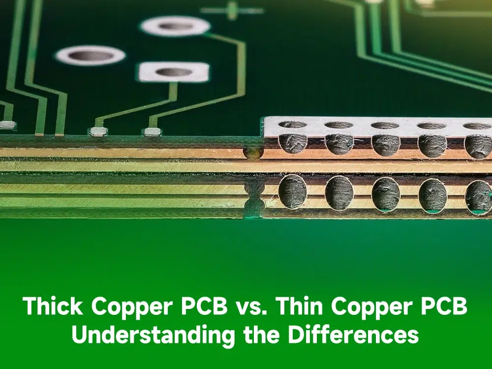
🔥 For high-current circuits, consider using heavy copper layers (e.g., 2oz or 3oz copper) instead of just increasing thickness.
Selecting the wrong PCB thickness can lead to manufacturing defects like soldering issues, excessive heat buildup, and even board warping under thermal stress. Engineers should consider the implications of heat dissipation and mechanical strength when deciding on PCB thickness. To avoid costly assembly errors, check out this list of the most common PCB assembly problems and their solutions in this article from Unit Circuits
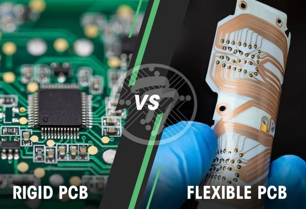
3️⃣ Mechanical Strength & Durability
If your PCB is exposed to shock, vibration, or mechanical stress, its thickness plays a key role.
💡 Thin vs. Thick PCB: Which One to Choose?
| Thickness | Use Case | Pros | Cons |
|---|---|---|---|
| 0.2mm – 0.8mm | Flexible & ultra-thin PCBs | Lightweight, space-saving | Fragile, limited durability |
| 1.0mm – 1.6mm | Standard PCBs (consumer electronics) | Good balance of rigidity & flexibility | Not ideal for high-current applications |
| 2.0mm – 3.2mm | Power electronics, industrial PCBs | Strong, good for high-current applications | More expensive, less flexible |
| 4.0mm+ | High-power, multilayer PCBs | Excellent durability & heat dissipation | Heavy, costly, longer manufacturing time |
Key Takeaway: If mechanical stress is a concern (e.g., automotive or aerospace applications), go for thicker PCBs. For flexible applications, thinner PCBs (even as low as 0.2mm) are ideal.
4️⃣ Manufacturing Constraints & Cost Implications
Not all PCB manufacturers can fabricate ultra-thin or extra-thick boards.
💡 Custom PCB Manufacturing with Any Thickness:
- Thin PCBs (<1mm): Require special lamination techniques
- Thick PCBs (>2mm): May have increased production time & costs
- Standard PCBs (1.57mm): Fastest & most cost-effective to produce
📌 Fast PCB Prototyping with Custom Thickness: Always check your manufacturer’s capabilities before finalizing a thickness specification.
Choosing a non-standard PCB thickness can increase production costs due to custom tooling requirements and material availability. Engineers should balance performance needs with cost-effective manufacturing practices. If you want to optimize your PCB design for better cost savings, check out this guide on reducing PCB assembly expenses from Unit Circuits: How to Save Money on PCB Assembly.
5️⃣ Application-Specific Needs
PCB thickness should align with your specific project requirements.
💡 What Is the Best PCB Thickness for My Project?
| Application | Recommended PCB Thickness | Reason |
|---|---|---|
| Wearable Tech | 0.2mm – 0.8mm | Flexibility, lightweight |
| Consumer Electronics | 1.0mm – 1.6mm | Standard, cost-effective |
| High-Speed Digital | 1.2mm – 1.6mm | Impedance control |
| Power Electronics | 2.0mm – 3.2mm | Heat dissipation, current carrying |
| Automotive & Aerospace | 2.0mm – 4.0mm+ | Mechanical strength, reliability |
3. Common PCB Thickness Standards & Layer Stack Considerations
Standard PCB Thickness Chart
| PCB Type | Common Thickness |
|---|---|
| Single-Layer PCB | 1.0mm – 1.6mm |
| 2-Layer PCB | 1.57mm (standard) |
| 4-Layer PCB | 1.57mm – 2.36mm |
| 6+ Layer PCB | 2.0mm – 4.0mm+ |
📌 Standard PCB Thickness for 2-Layer & 4-Layer PCBs: 1.57mm is the most commonly used thickness, but high-speed, high-power applications may require different thicknesses.
A standard PCB thickness chart helps engineers make informed decisions when designing circuits. Different applications require different stack-up configurations to balance impedance control, durability, and heat dissipation. You can find an in-depth analysis of these variations in this guide from Wevolver.
How to Choose PCB Thickness for High-Frequency PCBs
- RF & microwave designs often need 0.8mm – 1.2mm PCBs for better impedance matching.
- Thicker PCBs may require adjusted dielectric layer spacing for controlled impedance.
4. Industry Pain Points & How to Solve Them
🚨 Industry Pain Point: Many engineers struggle with balancing thermal, electrical, and mechanical properties when choosing PCB thickness.
💡 Solution: We offer custom PCB thickness options with optimized material selection, ensuring low MOQ PCB assembly for cost-effective production.
✅ Turnkey PCB Manufacturing with Optimized Thickness Selection: We help engineers prototype and manufacture custom-thickness PCBs with fast turnaround.
One common pain point in PCB design is that incorrect thickness selection can cause assembly challenges, such as warping, excessive solder bridging, or poor thermal performance. Following industry best practices for PCB manufacturing is crucial to ensure a smooth assembly process. You can learn more about the essential steps in PCB assembly in this guide from Unit Circuits.
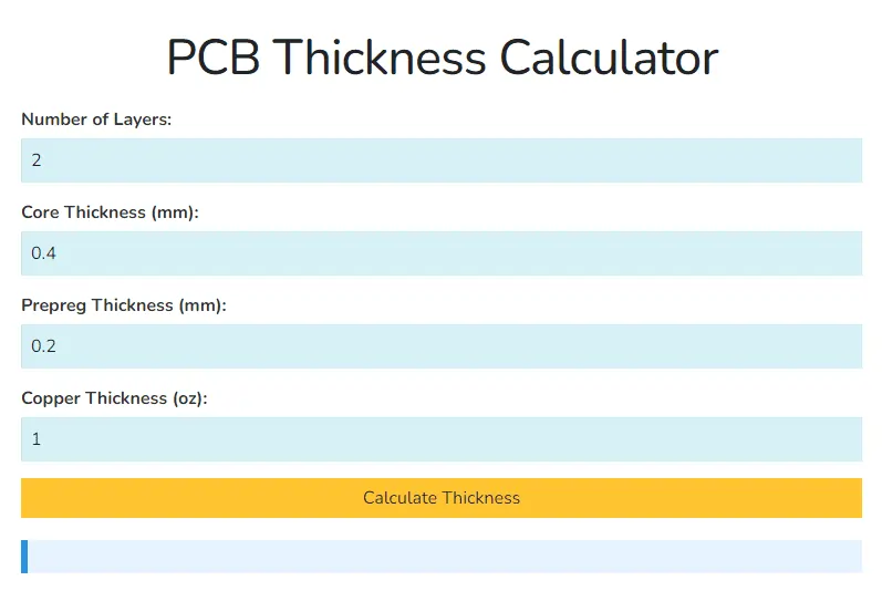
5. Quick Guide: How to Calculate PCB Thickness
PCB Thickness Calculator
A quick method to estimate thickness:
📏 Total PCB Thickness = Copper Layers + Dielectric Layers + Solder Mask
For a 4-layer PCB, you might have:
- Core Material (FR4, Rogers, etc.) → 0.8mm
- Prepreg layers → 0.2mm
- Copper layers → 0.035mm (each)
- Solder mask & silk screen → 0.05mm
➡️ Total PCB Thickness = ~1.57mm (standard)
If you’re unsure about the right PCB thickness for your project, online tools and calculators can simplify the process. Many manufacturers, such as ALLPCB, offer guidance on selecting custom PCB thicknesses for various applications. For more insights, check out this detailed article from ALLPCB.
FAQs
1.How to Decide PCB Thickness for My Project?
Choosing the right PCB thickness depends on factors like signal integrity, heat dissipation, mechanical durability, and manufacturing constraints. For high-frequency PCBs, thinner boards (0.8mm–1.2mm) improve impedance control, while power electronics benefit from thicker PCBs (2.0mm+). Standard PCB thickness is typically 1.57mm, balancing cost and performance. Use a PCB thickness calculator to determine the ideal stack-up for your circuit. If unsure, consult a custom PCB manufacturing service to optimize for low-MOQ PCB assembly and fast turnaround.
2.How Will You Determine PCB Size for Your Circuit?
The PCB size depends on component density, layer count, and mechanical constraints. Compact devices like wearables require small, thin PCBs (0.2mm–0.8mm), while industrial and power electronics need larger, thicker PCBs for heat dissipation. Consider PCB layout software to optimize routing and spacing. Using a standard PCB thickness chart helps maintain industry norms and reduces custom PCB manufacturing costs. If your design is complex, work with a turnkey PCB manufacturing service to ensure a high-quality, optimized layout.
3.What Are the Top 3 Important Steps in PCB Design and Layout Process?
- Component Placement & Routing – Optimize for signal integrity, heat dissipation, and manufacturability.
- Layer Stack-Up Selection – Choose the right PCB layer stack to balance impedance control, power distribution, and cost.
- DFM (Design for Manufacturability) Check – Ensure your design meets standard PCB thickness guidelines and can be manufactured efficiently.
💡 Tip: Use a custom PCB thickness calculator and collaborate with an experienced PCB assembly service to avoid costly revisions.
4.How Much Does PCB Design Cost Per Hour?
The cost of PCB design services varies based on complexity, experience, and location. Entry-level designers charge $30–$50 per hour, while experts handling high-speed, multilayer, or RF PCBs may charge $100+ per hour. Some turnkey PCB manufacturing companies offer low-MOQ PCB assembly with design support, reducing costs. If you're on a budget, consider fast PCB prototyping with custom thickness options to optimize production costs before mass manufacturing.
Have Specific Requirements?
Looking for high-precision PCB assembly for your products? Our team specializes in delivering top-tier assembly services, ensuring your devices perform flawlessly in any environment. Contact us today for a free consultation on how we can enhance your product’s reliability.
Conclusion
Choosing the right PCB thickness isn’t just about following a standard—it’s about optimizing performance, cost, and reliability.
🚀 Need expert help? Our custom PCB manufacturing services offer flexible thickness options, fast prototyping, and high-quality assembly.
📩 Get in touch today for a custom quote on your PCB design!
Save on your next PCB project?
Claim $100 OFF your order today.
✅ high-quality PCB assembly with strict quality control ✅ ISO-certified & 8+ years of experience. ✅ Low MOQ, fast turnaround, and 100% E-tested PCBs.
Additional Resources:
- How to Repair Circuit Boards: A Step-by-Step Beginner’s Guide
- Capacitor on Circuit Board: A Comprehensive Guide
- What Are PCB Conformal Coatings? Types, Benefits, and Applications Explained
- SMD Size Codes Explained: A Complete Guide to Understanding Surface-Mount Component Dimensions
- AC vs DC: Key Differences, Applications, and Advantages in Modern Electronics
Request for Quote
RECENT POSTS
IC Boards Explained: Applications, Layout Tips, and Assembly Services
Discover what IC boards are, how they’re used in modern electronics, and how to design
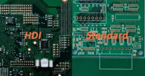
HDI PCB vs Multilayer PCB: How to Choose the Right One for Cost, Signal Integrity & Manufacturing
HDI PCB vs multilayer PCB explained from a manufacturing and assembly perspective. Learn how cost,
RELATED POSTS
Leading PCBA Manufacturer
✅ Assemble 20 PCBAS for $0 ✅ Get $100 OFF – Risk-Free Trial!
✅ 100+ Satisfied Customers
✅ Ensured Quality & On-Time Delivery
✅ Free Trial, No Commitments!