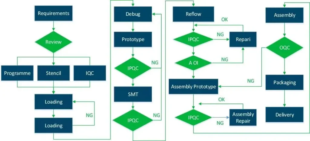
 ISO-certified & 8+ years of PCBA Low MOQ & Fast Turnaround Prototype & Mass production
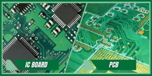
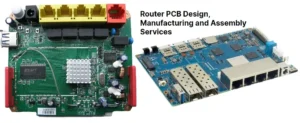
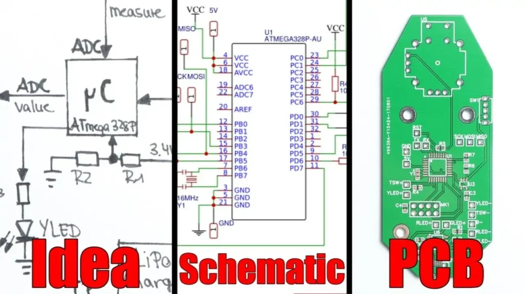
IC Boards Explained: Applications, Layout Tips, and Assembly Services
Discover what IC boards are, how they’re used in modern electronics, and how to design
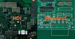
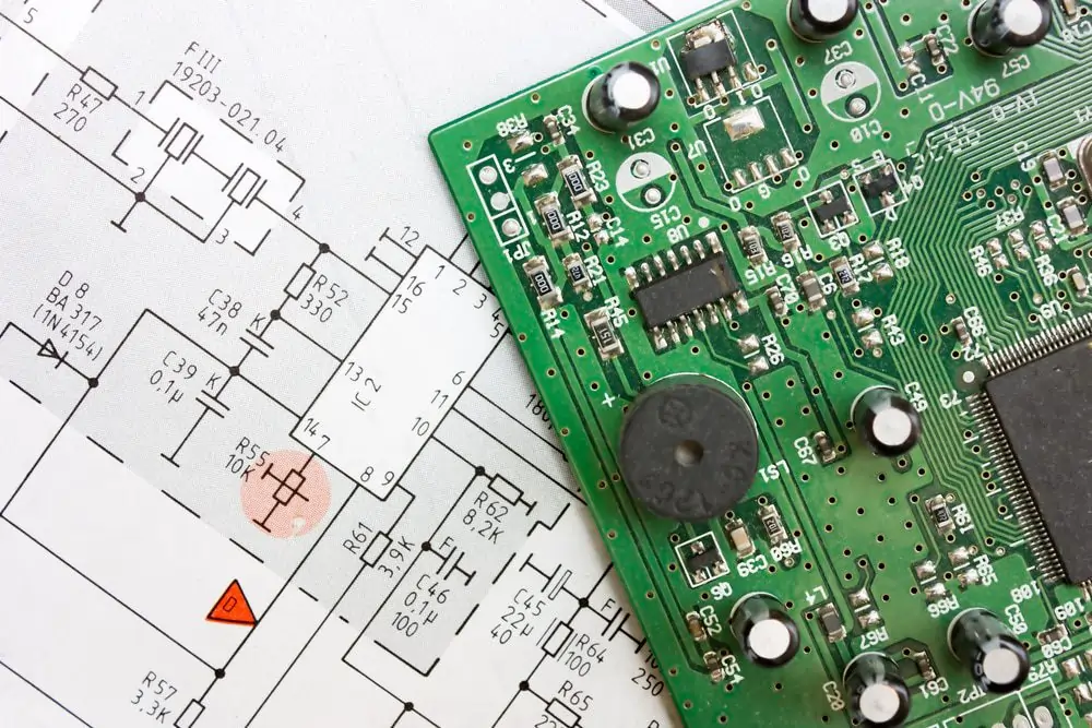
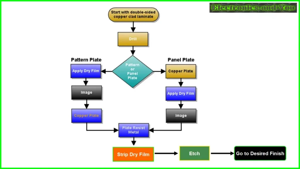
HDI PCB vs Multilayer PCB: How to Choose the Right One for Cost, Signal Integrity & Manufacturing
HDI PCB vs multilayer PCB explained from a manufacturing and assembly perspective. Learn how cost,