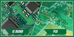
Quick Leads-PCBA
When you’re sourcing PCBs for high-reliability applications, the tiniest design detail—like whether a via is tented—can have big consequences. I’ve seen many assemblies fail because of overlooked via protection. So let’s talk about what tenting via actually is, why it matters, and how to get it right.
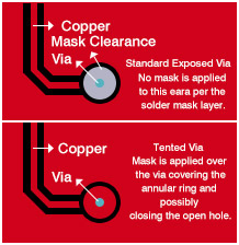
Tenting via is the process of covering a via’s annular ring and hole with solder mask during PCB fabrication. This creates a protective seal over the via, preventing moisture, debris, and solder from entering. Tenting vias is essential in protecting the circuit during surface mount assembly and reflow, improving overall PCB durability and reducing the risk of short circuits.
But here’s the thing—tenting isn’t always the best option. Let’s break down the when, why, and how of tenting, so you can make smarter design and sourcing choices.
What Is Tenting Via in PCB Fabrication?
If you’ve been in PCB design long enough, you’ve already encountered the term tenting via. But let’s clarify exactly what it is.
A via (Vertical Interconnect Access) connects different layers in a PCB. It’s essentially a small, plated hole that allows electrical signals or power to travel from one copper layer to another.
Tenting means applying solder mask over that via—both the hole and its annular ring—to seal it off from the environment.
This process is typically done during the PCB fabrication process, using Liquid Photoimageable (LPI) solder mask or dry film. Tenting helps with:
-
Preventing solder paste from wicking into vias during reflow
-
Avoiding accidental shorts
-
Reducing corrosion due to moisture or contamination
Vias that aren’t protected (or exposed) can become weak points in your PCB design, especially during high-volume or high-temperature processes.
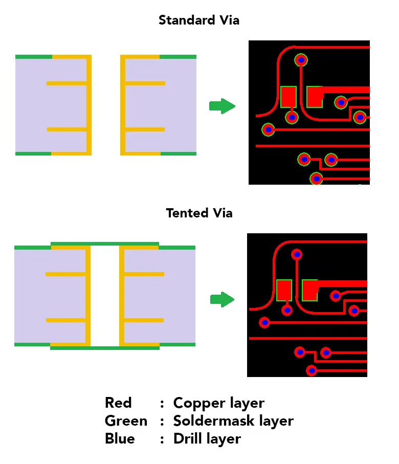
Types of Tenting and Common Techniques
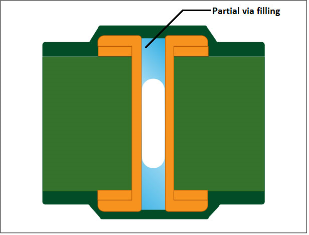
You’ll hear terms like fully tented, partially tented, plugged via, and filled via. Here’s what those mean in practical terms:
| Method | Description | Common Use Case |
|---|---|---|
| Tented Via | Solder mask covers the hole and pad; not guaranteed to be airtight | Consumer, low-cost boards |
| Plugged Via | Via is filled with non-conductive material; mask may be applied on top | BGA, HDI boards |
| Filled & Capped | Filled with conductive/non-conductive material and capped with copper | Via-in-pad, thermal dissipation zones |
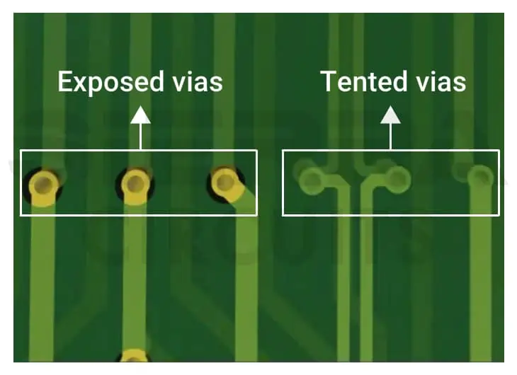
| Open/Exposed Via | No protection—via hole and ring are fully exposed | Debug/test points, RF tuning |
Tenting is the most cost-effective of the protection techniques, but it doesn’t offer as much mechanical strength or insulation as filled vias. If your design requires via-in-pad or high thermal conductivity, filled or capped vias might be more appropriate. Here’s a breakdown of PCB via filling techniques you might want to consider.
Unit Circuits: Leading PCBA Manufacturer
 ISO-certified & 8+ years of PCBA Low MOQ & Fast Turnaround Prototype & Mass production
Limited Time Offer:
Get $100 off your order TODAY!
Tenting Via vs Non-Tenting Via: Which One Should You Choose?
Let’s look at the pros and cons from a functional point of view:
| Feature | Tented Via | Non-Tented Via |
|---|---|---|
| Solder Paste Leakage | Prevented | High risk, especially near SMT pads |
| Contamination Risk | Low | Higher (open hole attracts debris) |
| Electrical Protection | Better isolation | Risk of shorts |
| Aesthetic Surface | Smoother | Exposed copper and hole |
| Manufacturing Cost | Lower | Slightly cheaper, but riskier |
When to use tented vias:
-
Around BGA pads (to prevent solder bridging)
-
On dense boards where you want a smooth finish
-
In high-moisture or high-contamination environments
When not to use them:
-
If you need the via as a test point
-
In high-frequency RF boards where impedance is critical
Via Tenting Design Rules and Best Practices
Here’s where many projects go off-track.
If your LPI solder mask isn’t aligned properly or your via size isn’t suitable, the tenting won’t fully seal. That can lead to:
-
Incomplete sealing → moisture ingress
-
Mask peel-off → reliability failures
-
Solder wicking → open or cold joints
Some quick design rules to follow:
-
Via size: Tenting works best on vias under 0.3mm (12 mil)
-
Annular ring width: 5–7 mils for clean mask coverage
-
Solder mask expansion: 3–4 mils beyond via pad
-
Spacing from SMT pads: Avoid placing vias too close to pads unless they are filled/tented
Also—check with your fabricator about minimum solder mask dam width. Not all houses can hold the same precision, especially for prototype PCB manufacturing. Refer to this in-depth via tenting rule guide from Sierra Circuits for a clearer understanding.
Common Problems in PCB Assembly Due to Poor Tenting
Even if your layout looks perfect, open vias can sneak in quality issues during assembly.
Here are the biggest offenders I’ve seen in practice:
-
Solder wicking: Paste flows into the via hole instead of forming a proper joint.
-
Open circuits: Especially around QFNs or BGAs, where paste escapes down un-tented vias.
-
Solder balling or bridges: Caused by uneven surfaces or exposed pads near vias.
We’ve also seen situations where vias under solder mask are partially exposed due to poor registration—which is worse than just leaving them open.
If vias are left open or only partially tented, they can cause reflow soldering defects like solder wicking or incomplete joints—especially under BGAs or QFNs. These issues often contribute to broader reliability challenges seen during PCB assembly. This article on common PCBA problems dives into more examples and how to prevent them.
Real Example:
A client once had 30% BGA failures on a prototype run. After inspection, we found tented vias underneath the pads were only half-sealed. Solder escaped into the via during reflow, leading to weak joints. After switching to filled and capped vias, the issue vanished.
How We Solve Industry Pain Points with Smarter Tenting Options
We don’t just “apply mask” and call it a day.
Here’s how we approach tenting at the manufacturing level:
-
Design-for-manufacturing (DFM) review: We flag problematic via sizes, placements, or spacing before fabrication starts.
-
Solder mask simulation: Our team runs optical previews to detect coverage risks.
-
Via choice guidance: If you’re near BGA zones, we recommend filled and capped vias.
-
Material options: LPI, epoxy-fill, or resin-filled for high-reliability needs.
We also offer via tenting in prototype PCB runs—so you can validate the design under real-world conditions before scaling. Choosing the right assembly partner means looking beyond price.
We’ve seen too many teams struggle with design files that weren’t DFM-checked or board houses that skipped key details like proper via tenting. Here’s a guide on what to look for when purchasing PCBA to avoid those headaches.
Fast-Turnaround, No-Min PCB Assembly—With Tenting Done Right
We know speed matters. That’s why we’ve integrated fabrication and assembly under one roof with:
-
Same-day DFM feedback
-
Quick quote + online gerber uploads
-
Assembly starting from 1 board (no MOQ)
-
Turnkey PCB assembly China-based with global logistics
If you’re building smart IoT, consumer electronics, or industrial devices—getting your via strategy right from Day 1 can save a whole lot of time and cost down the road.
FAQs
1. What’s the difference between plugged and tented vias in PCB design?
Tented vias are simply covered with solder mask, offering basic protection against dust and solder wicking. Plugged vias, on the other hand, are filled with a non-conductive material—usually epoxy—and often combined with capping for enhanced strength. If you're working with via-in-pad or high-reliability applications, plugged vias offer more structural and thermal stability. But for many standard designs, tenting vias remains a cost-effective solution.
2. Are tented vias more expensive than non-tented?
Not really—PCB via tenting is a minimal-cost process when compared to filled or capped vias. Most board houses already apply a solder mask layer, so covering the vias during that step adds almost no additional cost. In fact, by preventing rework and reducing assembly defects, tented vias often save you money in the long run. For cost-effective PCB solutions, tenting is a smart default.
3. Can you have too many vias on a PCB—and does it impact cost or reliability?
Yes, excessive vias can lead to signal integrity issues, heat dissipation problems, and increased fabrication cost. While vias are essential for multilayer routing, each one adds drilling time and complexity. High via density can also limit PCB prototype manufacturing options. Always balance performance with manufacturability, and consider via stitching or tented via techniques to reduce EMI while keeping your board cost under control.
4. What’s the purpose of via stitching and when should shielding vias be tented?
Via stitching involves placing multiple vias to connect ground planes, improving EMI shielding and heat dissipation. For shielded enclosures or high-speed signal paths, tenting shielding vias is often necessary to prevent exposure to moisture or accidental shorts—especially in humid or industrial environments. Combine this with grounded shielding to achieve optimal circuit integrity.
Have Specific Requirements?
Looking for high-precision PCB assembly for your products? Our team specializes in delivering top-tier assembly services, ensuring your devices perform flawlessly in any environment. Contact us today for a free consultation on how we can enhance your product’s reliability.
🧾 Summary
Tenting vias isn’t just about aesthetics—it’s a crucial reliability decision in modern PCB assembly.
Even if your PCB layout looks solid on screen, poor via coverage can lead to defects that only show up during final testing. That’s why thorough QA processes matter. Read about the top PCB assembly testing methods to see how issues like these are caught—and how to avoid them from the start.
Whether you’re prototyping or scaling up, understanding your via options means fewer surprises. Let’s talk—our engineers are here to guide your next design from layout to full production.
Save on your next PCB project?
Claim $100 OFF your order today.
✅ high-quality PCB assembly with strict quality control ✅ ISO-certified & 8+ years of experience. ✅ Low MOQ, fast turnaround, and 100% E-tested PCBs.
Additional Resources:
- How to Repair Circuit Boards: A Step-by-Step Beginner’s Guide
- Capacitor on Circuit Board: A Comprehensive Guide
- What Are PCB Conformal Coatings? Types, Benefits, and Applications Explained
- SMD Size Codes Explained: A Complete Guide to Understanding Surface-Mount Component Dimensions
- AC vs DC: Key Differences, Applications, and Advantages in Modern Electronics
Request for Quote
RECENT POSTS
PCB Transformer Explained: Types, Working Principle, and Design Tips
Discover how PCB transformers work, their key types, and design integration tips. Learn to select
Why Smart OEMs Avoid Cheap PCB Assembly: 5 Hidden Risks That Cost More
Avoid costly mistakes in OEM projects. Discover why cheap PCB assembly risks quality, compliance, and
RELATED POSTS
Leading PCBA Manufacturer
✅ Assemble 20 PCBAS for $0 ✅ Get $100 OFF – Risk-Free Trial!
✅ 100+ Satisfied Customers
✅ Ensured Quality & On-Time Delivery
✅ Free Trial, No Commitments!